diy solar

diy solar

Laying out and ordering PCBs

Cal

Solar Addict
Joined
Apr 28, 2020
Messages
752
What are the steps in designing/purchasing a PCB to build a BMS?

Do I need to generate a schematic? Which program/app? Does the schematic automatically routs traces on the board?

Where does one order boards? What are typical costs of a 4" x 2" board?
 
You should start by building BMS that has already gone down that route: https://github.com/stuartpittaway/diyBMSv4
He uses jlcpcb.com. I've ordered and received boards manufactured for me from jlcpcb for that BMS and will be putting the rest of the components on the board soon. JLCPCB does do SMD assembly but not through-hole so those have to be put on yourself. Biggest problem has been even some of the smd parts have been out of stock such as the attiny so you have to get those from other places and solder that on yourself as well. JLCPCB seems like one of the easier to use and cheaper places to get your boards made. Didn't take that long to receive the boards in the USA either.
 
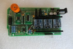
I already have a working breadboard. Don't have any CAD schematic drawing experience. What's a simple schematic program that will generate gerber files?

Breadboard.jpg
 
I have close to 50 years experience in electronics, 40 years owning my own company designing and servicing electronic equipment.

I can say even for me that designing and building my own BMS would be a huge undertaking. Even though I could do it, the cost and frustration level would not be worth the reward of "I did it myself because I can!". I'm new here I see there is an open-source project available above and myself I would go in that direction.

That said, when I design a new project, I start with a list of functions it needs to do. Then under each function I list the information and inputs/outputs I need to access to preform that function.

After I have a layout of all the steps, then on paper I sketch out a block diagram of the circuit. From there I start with the schematic... I used Eagle PCB because that is what I have used for 20+ years. Its not as fancy as some but I have not updated it in a few years, but it does autorouting of the PCB and I like that.

Once I have the schematic done and I've gone over all the processes in my mind, I layout the board and send it off to a PCB supplier for prototype service. Warning, you will find issues and will go through this process a few times. Be prepaired to spend a few hundred dollars on boards with errors. Now if I am making something simple and one-off for myself, I lay it out on a breadboard and get the circuit working. Then move the circuit onto a breadboard PCB.
 
I already have a working breadboard. Don't have any CAD schematic drawing experience. What's a simple schematic program that will generate gerber files?
EasyEDA enables to draw schematics right from the browser. There is nothing to install.
It should enable to generate PCBs as well, but i did not go that far:
Designing a PCB, especially for power or HF applications, is not something to improvise.
 
  • Like
Reactions: Cal
Your picture looks like a board for an Arduino Nano + many level shifters.
Why not considering directly a 3,3V microcontroller? I love the pro-mini 3,3V It has an extremely low consumption.
But now i went more on using the ESP8266 (Wemos D1) which provides WiFi connectivity.
That way I don't need a display/keys to operate.
 
I can say even for me that designing and building my own BMS would be a huge undertaking. Even though I could do it, the cost and frustration level would not be worth the reward of "I did it myself because I can!". I'm new here I see there is an open-source project available above and myself I would go in that direction.

I can understand that. I'm at a bit different orientation. I took an early retirement from electronics some 23 years ago to peruse camping and mountain biking the best trails in the western US. I'm now at an age where my body doesn't respond well to steep mountain climbs. Some of my (new) spare time is now taken up with Arduino projects. What an amazing product! Wish it was around 50 years ago.

Yeah, it's a lot cheaper to purchase a BMS. I'm currently using a Chargery BMS. I like the Chargery concept, but feel performance can be improved. Guess you can call it a new hobby; to build a better BMS. Hobbies are never cheap.

@rin67630 I'm using a ESP32 in order to use WiFi. That's another great advancement for processors. The processor plugs into the breadboard on top of the level shifters. The two multiplexers and ADC that are used need a 5V signal; hence the level shifters.

What if I want to install the level shifter modules in the new circuit board? Will the schematic generating program have this part listed or do I need to create a "custom" part?
There is a very good chance that all your components will be available in the KiCad libraries.
 
  • Like
Reactions: Cal
I'm a professional EE and second the opinion for KiCAD. At work we typically use Altium or ConceptHDL+Allegro, but those are expensive for a hobbyist and that would be nuts for someone making their first board. 10 years ago the hobbyist standard was Eagle, but KiCAD is now better and Eagle got sold to AutoDesk who killed off the free version.

Having said that, I don't think you're going to save any money compared to an off-the-shelf BMS and yours will certainly perform worse. It requires some skill and experience to design circuits (and often a technical degree to do good design) and you aren't going to get a great result on your first go around. But, if this is more for hobby purposes and not something you rely on to not burn down your house, well you have to start somewhere. So in that case it seems like a great hobby project to learn about PCB design!

I have also used KiCAD + JLCPCB for some smaller projects, and it's generally fine for basic stuff. The price is incredible. In the last few years, JLCPCB added an inventory of about 10,000 components which if you stick to using only them, they can also do the assembly for you! You should consider doing that rather than assemble your board yourself. If you need a couple components not on their list you can still get it mostly assembled and save yourself a lot of trouble with SMT soldering / DIY reflow. I've done some solder-screening and reflow too for prototypes and can answer some questions if you have any.

It's been several years since I learned KiCAD, but I think I watched some YouTube video to get oriented; it may have been this one:
 
Last edited by a moderator:
A few more comments:

Your breadboard prototype layout and assembly looks nice and clean, so it looks like you have the aptitude to do good PCB layout. You just have to learn about it: wire/via sizes, copper regions/pours/planes, footprints/symbols, floorplanning, etc.

If you're using a schematic from someone else who has already done the design that makes it easier since you just need to do the layout. Or, if you want me to review your schematic for issues I could try to do that. I haven't designed a BMS myself but think I understand the concepts.

I recommend Digi-Key for all your parts, or, at least for those not provided by JLCPCB if you choose to get it assembled by them. Mouser would be my second choice but those are the top 2 by market share and EE mind-share. You can try Octopart.com too but generally if it isn't sold by Digi-Key or Mouser you should reevaluate whether that component should be used in your design.
 
Last edited by a moderator:
  • Like
Reactions: Cal
A lot of the PCB providers also have a design service from your schematic. You specify key component placement such as connectors and they do the rest.

They do a really good job as all they do daily and as the layout is impacted by the PCB process when you get to more advanced designs you get a much better product.

I'd see if this is offered.
 
Having said that, I don't think you're going to save any money compared to an off-the-shelf BMS and yours will certainly perform worse. It requires some skill and experience to design circuits (and often a technical degree to do good design) and you aren't going to get a great result on your first go around.

You're giving off-the-shelf BMS too much credit. Chargery (BMS) current measurement couldn't be much worse. It neglects any charge or discharge current less than 1A. Current granularity is 250 mA for a 300A shunt. I know I can to better than that. Hence my project.

ah-over-25-hrs-jpg.23541


The chart shows after 17 hours, Chargery coulomb count is off by almost 15 AH! What the heck?

My BMS has a current granularity of 6 mA with a 300A shunt. A significant improvement over 250 mA! Yes, I can do lots better.
 
You're giving off-the-shelf BMS too much credit

Yeah, fair enough. I meant more in the way that your first PCB is likely to have design and implementation issues. It may take some iteration and learning to produce something that works well in all cases. But, it sounds like you know what you're doing. I'd love to look at your schematic if you want to post it to Github or here.

Can you link to the Chargery parts you're trying to replace? It looks like your breadboard is missing a whole bunch of high-current MOSFETs and heatsinks for conducting the current of the battery. Maybe you're designing something that just monitors the battery's state of charge but doesn't protect it? I think this would be more of a battery monitor or a shunt monitor than a battery management system.

For shunt monitors the gold standard right now is the TI INA series, specifically the INA229 I think is the latest and greatest one:

 
Last edited by a moderator:
By the way zero doubt you can do better than a China BMS.

Also look at Analog Devices - they have some very interesting "grid" BMS chips for use in smaller packs such as in a cell phone to get max runtime out of them. Not sure how to scale that design up but having individual full charge/discharge control on a cell level is certainly the way to optimize the pack fully with still maximum safety. Just don't know if it can be done above a couple Ah pack size reasonably yet.
 
  • Like
Reactions: Cal
Still not totally sure what you're building, but just as a "best case" comparison with the INA229 and the Chargery 300A shunt:

300A * 0.25mOhm / 312.5nV step size = 240k steps, so your resolution would be 1.25mA. You would have to use the larger ADC range for this particular shunt, on the INA229, to reach the full scale current of the shunt without saturating the ADC.

The chargery 300A shunt is only 0.5% accurate, which is 750mA at half-max. But if you calibrate it using a large and known current you can probably reduce that error source significantly. Obviously the calibration residual is the main thing to figure out, as the uncalibrated error is roughly 600x the size of the INA229 resolution! I bet the same is true of the electronics you're using, although I'm pretty sure they are not as good as the INA series. It's a cutting edge 20b ADC with an integrated low-offset front end, and I believe it is the best you can do with off the shelf parts.

Having said that, it looks like you're trying to reduce the low-load error by improving the resolution. So at ~25mA (10x better than the 250mA resolution that's a problem), the 300A shunt produces a 6.25uV voltage. At this low of a signal, you need to worry about everything on the board and in the shunt, including temperature gradients causing error voltages from dissimilar metals (ex: where your copper wires connect to your tinned circuit board). It means you really do need something like the 2uV-offset INA229 or other extremely-low-offset analog front end, in order to really do much better in these low-current cases.

Source: INA229 datasheet, and my experience designing low-offset analog integrated circuits at work.

Edited a few times; refresh for the latest.
 
Last edited by a moderator:
  • Like
Reactions: Cal
I'm getting 6 mA resolution with an INA226. A very nice part! It is located next to the 300A shunt. I like the Chargery architecture where the BMS only provides a signal for over-voltage or under-voltage disconnect. There are no power fets on this board.

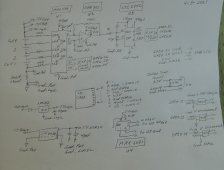
Here's a hand drawn schematic of the circuit. Presently I have no knowledge of computer drawn schematics. Back in the "old days" we had drafts people that did the drawings. Though I do recall drawing some schematics on mylar myself.

This schematic is actually my second attempt at a BMS. I got everything working on the first design (each cell had its own voltage divider and cell voltages are calculated by subtracting voltage divider measurements), but the thermal drifts were extremely bad. A new design was needed. 75% of the new design (cell voltage measurement) is lifted from @BiduleOhm BMS. He has a much better grasp of modern technology than I do.

The BMS contains a SD card connector for data logging, multiple Dallas Temp sensors, 4N35 optocouplers to provide battery disconnect signals, and a connector for the INA226 signals.

BMSschematic.jpg
 
To answer the first questions quickly I use KiCad and allpcb as the manufacturer.

What if I want to install the level shifter modules in the new circuit board? Will the schematic generating program have this part listed or do I need to create a "custom" part?

If the part isn't in the default libs you may be lucky and be able to download it (either on the mouser/digikey page of the component or by searching on google the component ref + kicad), be warned that managing those files is a bit of a PITA with KiCad, I recommend you follow this: https://hackaday.com/2017/05/18/kicad-best-practises-library-management/ if you can't find the component then you'll have to make it yourself, it's not that complicated, there's nice tutorials on youtube ;)

Also, a nice trick is to copy an existing component who is close to yours and make the changes needed as it'll make you gain a lot of time.


Do I need to generate a schematic? Which program/app? Does the schematic automatically routs traces on the board?

The order is to make the schematic, then route the PCB, then export the gerber files, check them with an independent gerber viewer (there's some free online ones, don't even need to install anything) which is a very important step since it's the last chance you have to spot errors before PCB are made, then send the files to the manufacturer and wait ;)

There's a pretty high chance your first PCB(s) will have big mistakes and you'll have to make a new revision, so try to stay small and simple for your first PCBs (your current project should be simple enough as a first PCB).

I recommend this serie of videos:
it's maybe a bit too much in depth but I never saw better videos on that subject yet so yea... just ignore things related to panelization for example.

PS: yes, I'm still alive, just super busy right now; it should get better in the weeks to come hopefully...
 
Last edited:
Cool stuff @Cal ! This looks good, but I have some comments anyway if you want to think about them. I'll adjust my comments to a higher level since you are clearly an above-average forum user with respect to circuits. I apologize if any of my prior comments were patronizing, I just assumed a certain level based on you asking for advice about using PCB software.

- You're already using an INA part for the shunt; that's good. The last one I used was the INA219, but a colleague of mine recently used the INA226. That's a good choice and will work very well for your 300A shunt.

- Sigma-delta ADC is a good choice as bandwidth is not important and you don't want something more difficult to drive, like a SAR ADC.

- OPA991 is reasonably low offset (125uV). You can definitely go lower-offset with a chopper amplifier, typically 10uV. In integrated solutions like inside the INAs, the chopping is synchronous to the ADC sampling. But, 125uV is probably ok for this application. More on this later.

- You may as well add a capacitor in the feedback loop of the op-amp circuit to further reduce its bandwidth and noise, since you don't need to maximize bandwidth in this application.

- Your op-amp circuit is single ended. A better solution since you have a differential sensor, a differential MUX, and a differential ADC, would be to also use a fully-differential amplifier. These have a common-mode feedback loop which keeps the output common mode constant even as the input differential mode (and common mode) is varying. I can expound on this if you're interested**; but long story short you should replace the resistors and op-amp with something like this:

- The mux's resistance and the input resistors for each of its 8 paths will add to your gain error since it participates in the R2/R1 gain of the op-amp circuit. Ideally you would not have this source of error since it would use matched resistors on the opposite side of the mux. Assuming you stick with a discrete approach like this, you should at least move the resistors to the opposite side of the mux (which also eliminates the need for some of them). If you instead switch to the fully-differential topology I linked to above, the resistors are now integrated and matched for you inside the amplifier silicon, and you just have MUX -> DIFF_AMP -> ADC, fully differential the whole way, with no discrete resistors to worry about.

- Similarly, you'll get better resistor matching if all 100k resistors are in a single package, as they are on a single integrated circuit, typically better than if you're using discrete 0.1% resistors like you did in your prototype design. The actual value is not important, only the matching is important.


**Ok, a little expounding is in order: Right now you're relying on the input common mode rejection of the OPA991 which is a less optimal way to reject the varying common mode as you move up the stack of batteries with your MUX. You're also introducing a differential-mode to common-mode error at the ADC, since you're using a differential ADC in a single-ended mode. A reason to change it how I described above is because offset voltage and gain error are both common-mode-voltage dependent (in both the op-amp and the ADC). A second reason is that differential signaling is less susceptible to outside interference than single-ended signaling. On-chip stuff is fully-differential the whole way, typically.

Source: I interned at Analog Devices for a year while in grad school and designed a low-offset fully-differential amplifier, before starting my actual career in this field. Seems pretty apropos to the circuit at hand!

Edited a few times after initial writing.
 
Last edited by a moderator:
Back
Top