diy solar

diy solar

DIY BMS design and reflection

Why care about Rjc? The ultimate goal is to calculate junction temperature. Even if the value is small, it's an essential component for thermal flow: junction-to-case-to-heatsink-to-ambient. The starting point (ambient temp) and the end point (junction temp) should be documented in the thermal equation. Minor impedances in-between can be neglected for the sake of simplicity.

Ok, but the PCB Rth is around 1 °C/W in this case, so it is not minor and is actually a lot more essential than the MOSFET Rjc which is only 0.35 °C/W.


Perhaps you haven't understood my question. How do you prevent the body diode from conducting load current in a single port system when a over-voltage fault is active? In other words, charging is disabled, but load current is enabled.

Oh ok, I see. I don't enable one without enabling the other so I don't have this problem.
 
Ok, but the PCB Rth is around 1 °C/W in this case, so it is not minor and is actually a lot more essential than the MOSFET Rjc which is only 0.35 °C/W.


Oh ok, I see. I don't enable one without enabling the other so I don't have this problem.

Is the PCB located between the fet and heatsink? I didn't realize that.

If you don't enable one fet without enabling the other during fault conditions then in all probability you are implementing the design discussed by Pidjey. N'cest pas?
 
Is the PCB located between the fet and heatsink? I didn't realize that.

Yep ;)


If you don't enable one fet without enabling the other during fault conditions then in all probability you are implementing the design discussed by Pidjey.

Not sure about which design you're talking about exactly, but I'm implementing a standard bidirectional switch based on MOSFETs with a common source topogoly.
 
  • Like
Reactions: Cal
https://diysolarforum.com/threads/i-want-to-make-my-own-bms.17003/post-200065
You state: "Unless you use a separate ports design the body diodes (or external ones) will be used, no way around that."

I'm a bit confused. Here you state the body diode will conduct during a fault condition (now way around that).

As it turns out, there is a way around the problem. Monitor current and activate gate drive to the fet who's body diode is conducting.
 
Yes, but only if you want separate charge and discharge disconnection. Basically doing separate port features but with a common port topology.

Yep, I didn't thought about that solution at that time but it should work ;)
 
Last edited:
I've decoded the Schneider Modbus protocol and written some very rudimentary Python code to set the SCC and Inverter into STDBY/ONLINE as well as getting statistical data using Modbus TCP (but I could easily add RS-485 as layer 1 instead of TCP.) For Schneider, you have to have the Conext Gateway to achieve communication since they keep Xanbus pretty close to the vest. Given the specs for other mfgs, I could probably code that functionality as well. If your interface board can run a higher level programming language or even C, I could lend a hand with the communication.
Would you mind sharing your Python code? Having a RasPi to shutdown the CC/Inverter gracefully is much prefered then the BMS being brutal.
 
Would you mind sharing your Python code? Having a RasPi to shutdown the CC/Inverter gracefully is much prefered then the BMS being brutal.
Sure thing. Make sure you enable Modbus TCP on your Conext Gateway and edit the code to put in your Conext Gateway's correct IP Address. Mine is shown in the code as an example.

The code below only queries the Modbus device. I did all of updating of registers manually in the Python console (shown in the Modbus notes) and you'll need to remember the port is different when writing to registers (it's 503 "slave port" compared to 502 which is using the master port - on Gateway.) Here's the docs for "pyModbusTCP" python module:

If you want to modify a register (disable charging on CC,) you'll need to use the "write_single_register(reg_addr, reg_value)" function.

So it's a little complicated if you're not used to type conversions. I've attached my notes for registers I've found useful to query/set. Here's the query code and an example execution querying the inverter for DC Bus Voltage. You need to use command line args to assign the "port" the Conext Gateway is using for Modbus TCP, the "unit_id" of the device you want to query, and the "reg"ister you want to retrieve or update:

#!/usr/bin/python3 from pyModbusTCP.client import ModbusClient from time import sleep import sys, getopt # Default data type data_type = "uint16" try: opts, args = getopt.getopt(sys.argv[1:],"hp:u:r:t:",["port=","unit_id=","register","type"]) except getopt.GetoptError: print('query.py -p <port> -u <unit_id> -r <register> (-t <type> | default=uint16)') sys.exit(2) for opt, arg in opts: if opt == '-h': print('query.py -p <port> -u <unit_id> -r <register>') sys.exit() elif opt in ("-p", "--port"): port = arg elif opt in ("-u", "--unit_id"): unit_id = arg elif opt in ("-r", "--register"): reg = arg elif opt in ("-t", "--type"): data_type = arg if not port or not unit_id or not reg: print('query.py -p <port> -u <unit_id> -r <register> (-t <type> | default=uint16)') sys.exit() print("port: {}".format(port)) print("unit_id: {}".format(unit_id)) print("reg: {}".format(reg)) print("type: {}".format(data_type)) client = ModbusClient(host="192.168.0.152", port=port, auto_open=True, auto_close=True, debug=False, unit_id=unit_id, timeout=30) # Setup registers with ADDRESS,REG_COUNT,TYPE # Address: reg_count (uint16: 1, uint32: 2, str16: 8, str32: 16) reg_dict = {} reg_count = 1 reg_type = "uint16" reg_count = 1 if reg_type == "uint32": reg_count = 2 if reg_type == "str16": reg_count = 8 if reg_type == "str20": reg_count = 10 if reg_type == "str32": reg_count = 16 #print("reg:{} reg_count:{}".format(reg, reg_count)) #print("reg:{} reg_count:{}".format(type(reg), type(reg_count))) hold_regs = client.read_holding_registers(int(reg), reg_count) sleep(0.5) input_reg = client.read_input_registers(int(reg), reg_count) sleep(0.5) discrete_reg = client.read_discrete_inputs(int(reg), reg_count) relay_reg = client.read_coils(int(reg), reg_count) #print("holding_registers addr:{}".format(reg)) print("hold_register: {}".format(str(hold_regs))) print("input_register: {}".format(str(input_reg))) print("discrete_register: {}".format(str(discrete_reg))) print("relay_register: {}".format(str(relay_reg))) """ last_reg = 1 while last_reg <= 84: test_regs = client.read_holding_registers(int(last_reg), 125) print("test_register: {}".format(str(test_regs))) last_reg = last_reg + 1 """


$ ./query.py -p 502 -u 1 -r 40278
port: 502
unit_id: 1
reg: 40278
type: uint16
hold_register: [5225]
input_register: [5225]
discrete_register: None
relay_register: None
 

Attachments

  • ModBus notes.pdf
    21.7 KB · Views: 8
Last edited:
Sure thing. Make sure you enable Modbus TCP on your Conext Gateway and edit the code to put in your Conext Gateway's correct IP Address. Mine is shown in the code as an example.

The code below only queries the Modbus device. I did all of updating of registers manually in the Python console (shown in the Modbus notes) and you'll need to remember the port is different when writing to registers (it's 503 "slave port" compared to 502 which is using the master port - on Gateway.) Here's the docs for "pyModbusTCP" python module:

If you want to modify a register (disable charging on CC,) you'll need to use the "write_single_register(reg_addr, reg_value)" function.

So it's a little complicated if you're not used to type conversions. I've attached my notes for registers I've found useful to query/set. Here's the query code and an example execution querying the inverter for DC Bus Voltage. You need to use command line args to assign the "port" the Conext Gateway is using for Modbus TCP, the "unit_id" of the device you want to query, and the "reg"ister you want to retrieve or update:

#!/usr/bin/python3 from pyModbusTCP.client import ModbusClient from time import sleep import sys, getopt # Default data type data_type = "uint16" try: opts, args = getopt.getopt(sys.argv[1:],"hp:u:r:t:",["port=","unit_id=","register","type"]) except getopt.GetoptError: print('query.py -p <port> -u <unit_id> -r <register> (-t <type> | default=uint16)') sys.exit(2) for opt, arg in opts: if opt == '-h': print('query.py -p <port> -u <unit_id> -r <register>') sys.exit() elif opt in ("-p", "--port"): port = arg elif opt in ("-u", "--unit_id"): unit_id = arg elif opt in ("-r", "--register"): reg = arg elif opt in ("-t", "--type"): data_type = arg if not port or not unit_id or not reg: print('query.py -p <port> -u <unit_id> -r <register> (-t <type> | default=uint16)') sys.exit() print("port: {}".format(port)) print("unit_id: {}".format(unit_id)) print("reg: {}".format(reg)) print("type: {}".format(data_type)) client = ModbusClient(host="192.168.0.152", port=port, auto_open=True, auto_close=True, debug=False, unit_id=unit_id, timeout=30) # Setup registers with ADDRESS,REG_COUNT,TYPE # Address: reg_count (uint16: 1, uint32: 2, str16: 8, str32: 16) reg_dict = {} reg_count = 1 reg_type = "uint16" reg_count = 1 if reg_type == "uint32": reg_count = 2 if reg_type == "str16": reg_count = 8 if reg_type == "str20": reg_count = 10 if reg_type == "str32": reg_count = 16 #print("reg:{} reg_count:{}".format(reg, reg_count)) #print("reg:{} reg_count:{}".format(type(reg), type(reg_count))) hold_regs = client.read_holding_registers(int(reg), reg_count) sleep(0.5) input_reg = client.read_input_registers(int(reg), reg_count) sleep(0.5) discrete_reg = client.read_discrete_inputs(int(reg), reg_count) relay_reg = client.read_coils(int(reg), reg_count) #print("holding_registers addr:{}".format(reg)) print("hold_register: {}".format(str(hold_regs))) print("input_register: {}".format(str(input_reg))) print("discrete_register: {}".format(str(discrete_reg))) print("relay_register: {}".format(str(relay_reg))) """ last_reg = 1 while last_reg <= 84: test_regs = client.read_holding_registers(int(last_reg), 125) print("test_register: {}".format(str(test_regs))) last_reg = last_reg + 1 """


$ ./query.py -p 502 -u 1 -r 40278
port: 502
unit_id: 1
reg: 40278
type: uint16
hold_register: [5225]
input_register: [5225]
discrete_register: None
relay_register: None
Perfect, thanks very much!
 
Answering here to this post.

Hi,

I need to understand, how mosfet is selected for BMS application.
It will be helpful if you share the equations you used to select mosfet for voltage. SC current, Temperature etc.

Well, it's a complex problem I can't really sum up in a post but I'll try anyway (please note that if you want to select a MOSFET for this application for real you need to learn more about that subject, this post will probably not be enough) :)

First you need to determine the minimum rated Vds(max) you'll need. Here it's not too complicated as the battery will never go over 64 V (for 16S LFP and 14S NMC) so the standard Vds(max) directly above that is 80 V. Ideally you want more margin than that for various reasons but mainly so you can have TVS diodes to catch the inductive spike when you turn the MOSFETs off (they are basically robust zener diodes so you need some margin for them to not conduct at 64 V and to fully conduct before hitting the MOSFET Vds(max) voltage) and 16 V is barely enough so a 100, 120 or 150 V MOSFET would be better.

But there is a big trade-off with higher voltage MOSFETs: they also have a higher Rds(on) (all other things being equal) which means higher losses. You can always throw more money to solve the problem (mainly better MOSFETs and/or more MOSFETs in //) but in my case I have very tight constraints regarding budget, thermal design, etc... so that's why I selected a 80 V MOSFET instead of a 100+ V one. By now I guess you start to realize (if you didn't knew already) that selecting a MOSFET is basically a big heap of compromises ?

Speaking of the Rds(on) it's the next big thing you'll need to choose. Lower = less losses but of course = more expensive (and the relation isn't linear; the cost will far more than double if you want half the Rds(on)...) so that's why usually it's a better idea to have multiple MOSFETs in // instead of only one super low Rds(on) MOSFET. Multiple MOSFETs is also an advantage for thermal reasons as you have more surface area to transfer heat to a heatsink and they can be spreaded too. Note that MOSFETs in // must be closely thermally coupled (i.e. being on the same heatsink) to avoid problems with current sharing due to varying Rds(on) with the Tj.
Also, you need to use the worst case (or at least real world) Rds(on) and not the big number at the top of the datasheet if you don't want your MOSFETs to melt. For example the MOSFET I chose is advertised as 1.1 mOhm but that's the typical value at Tj = 25 °C... the typical value at Tj = 120 °C is 1.9 mOhm and the max is 2.4 mOhm, which is more than double and of course that means more than double the losses and heat to disispate.
Also, don't select the MOSFET based on its Id(max) as in our application the Rds(on) and so the thermal limit will be reached far before the Id(max) gets relevant (for example I use MOSFETs with a Id(max) of hundred of amps each but I only pass 30 A per MOSFET as the Tj would get too high with more than that).

Then we enter the "details" and it can get complex but they are important if you don't want to fry the MOSFETs the first time they turn on or off, or even by just connecting them to the battery and loads...

If you want to be capable to make an e-fuse feature and so be capable of interrupting a short-circuit safely you'll need to turn the MOSFETs off very quickly (single digit µs maximum, else they'll melt...) and that includes the total delay (detecting that the current is too high, driving the MOSFET gate, etc...), not just the MOSFET turn off time you can find in the datasheet. That means hardware only (software will be too slow unless you have a very very fast MCU which you will not since it's a BMS, not a PC), no low-pass filter, fast amplifier, fast comparator, very good gate driver, very low gate resistance, low inductance routing, etc...
Of course you also need to check that the maximum expected short-circuit current (usually a few kA for most of our systems) is below the Id(max) of the MOSFET by a good margin (current that high will not share as equally as the normal current between the MOSFETs), you'll need to use the appropriate graph in the datasheet as the table will not be enough since it's dependent on time.
NB: if you don't implement an e-fuse then be ready to accept loss of the MOSFETs if there's a short-circuit as a classic fuse will be far too slow to protect them.
NB²: an e-fuse doesn't replace a classic fuse (unless it's triple redundant and certified, which will not be the case here), always include a classic fuse in your system for the "you never know" case.

Another very important thing is the PCB layout as you must ensure that the PCB traces can handle the expected current (I plan to add busbars for example as 300 A is to much, even with a 8 layers PCB...) and you also need to share the current as equally as possible if you use multiple MOSFETs in //. And, of course, you need to do all that while still having a proper heatsinking strategy. Also, 64 V isn't high but it's not low either, you must pay attention to clearance and creepage distances.

Another thing to take into account is that the MOSFETs can turn on if there is a high enough dV/dt between their drain and source (when you physically connect the BMS to the battery for example) even with a pull-down resistor on their gate, that's because there is parasitic capacitances between the gate and the drain, and the gate and the source (and also between the drain and the source but we don't care about that here), more info here. They form a capacitive divider which will divide Vds by a ratio equal to Crss / Ciss and if this voltage is over Vgs(th)(min) then the MOSFET will turn on.
Now the obvious and easy thing to do to fix that is to add a capacitor big enough between the gate and the source so the divider ratio gets big enough that Vgs is never high enough to turn on the MOSFET. Small problem with that: the gate driver will have to charge and discharge this additional capacitance and it'll greatly increase the turn-on and turn-off times, the former isn't a big problem but the later is if you want the e-fuse feature described earlier.
The best solution I found is to add schottky diode so the capacitor doesn't increase the turn-off time (it still increases the turn-on time but it's way under the maximum we could want for it so we don't care here):
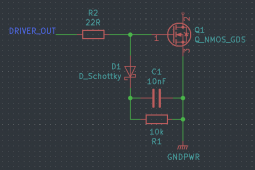
mosfet.png

Note that the values are placeholders. You need to calculate C1 via this formula: C1 = Crssmax * (Vdsmax / Vgsthmin) which in my case gives C1 = 1.7 * (64 / 1.2) = 90.7 = 100 nF (you need to use worst case for Crss(max) and Vgs(th)(min) and in my case I had to use the graphs as the table in the datasheet didn't give those). R1 isn't super critical and anything around a few dozen kOhm is fine. The diode must have the lower Vf possible. Regarding the PCB layout, C1 and D1 must be as close to the MOSFET as possible with traces of as low inductance as possible.

NB: I haven't tested my design IRL yet so even if I always use the worst cases and add some margin to be safe, some of what I described above might not be enough to not fry the MOSFETs in some extreme cases.


Side note unrelated to all that MOSFET stuff but related to the projet itself: I had to pause working on it for quite a few reasons but I resumed working on it since a few days. I'm currently selecting the LEDs for the HMI board and then I'll route the PCB for it (the schematic was already finished from before).
 
Last edited:
Answering here to this post.


Well, it's a complex problem I can't really sum up in a post but I'll try anyway (please note that if you want to select a MOSFET for this application for real you need to learn more about that subject, this post will probably not be enough) :)

I have been designing power electronics for a long time and MOSFET selection seems to get a little more challenging for each design since I learn a little more about the FETs every pass. I commend you for writing a summary of decision matrix. It is a very complex topic and it very rarely ends with a clear decision.

It also gets rather consequential as the current and voltage increase where a minor 'oops' becomes a bigger and bigger problem. A 12v / 10A switch will smoke a little when you mess up. A 48V / 300A switch gets pretty messy in the presence of poor decisions.
 
Another thing to take into account is that the MOSFETs can turn on if there is a high enough dV/dt between their drain and source (when you physically connect the BMS to the battery for example) even with a pull-down resistor on their gate, that's because there is parasitic capacitances between the gate and the drain, and the gate and the source (and also between the drain and the source but we don't care about that here), more info here. They form a capacitive divider which will divide Vds by a ratio equal to Crss / Ciss and if this voltage is over Vgs(th)(min) then the MOSFET will turn on.


View attachment 70422

I never heard of mosfets turning themselves on when applying battery voltage. Then again, I've left work over 22 years ago. What I recall is that it's rather difficult to turn the mosfet on. It takes quite a bit of energy. A negative feedback phenomena occurs as the fet is turning on. For the fet to turn on, the gate-drain capacitance (Cgd) gets charged to about 10V. This capacitance is quite small, but the capacitance gets multiplied by the gain of the fet. Cgd is called the Miller capacitor, Its capacitance increases by the gain of the fet. Now this capacitor becomes very large and it takes a lot of energy to charge it. A high current source is needed to charge Cgd and quickly switch the fet. That's why R2 is only 22 ohms.

As I see it, when battery voltage is applied to the Cgd and Cgs voltage divider, Cgd is charged by the opposite voltage polarity from what's required to turn the fet on. I don't see how the fet can turn on without first depleting this charge and then charging the capacitor to 10V (or more exactly fet threshold voltage).
 
What I recall is that it's rather difficult to turn the mosfet on. It takes quite a bit of energy.

It doesn't take a lot of energy (E = 0.5 * C * V² which in my case gives 0.5 * 13 * 10^-9 * 64² = 27 µJ) but it takes quite a lot of current with a high dV/dt (but our batteries can supply multiple kA easily and connecting a lug creates a high dV/dt).

A negative feedback phenomena occurs as the fet is turning on. For the fet to turn on, the gate-drain capacitance (Cgd) gets charged to about 10V. This capacitance is quite small, but the capacitance gets multiplied by the gain of the fet. Cgd is called the Miller capacitor, Its capacitance increases by the gain of the fet. Now this capacitor becomes very large and it takes a lot of energy to charge it. A high current source is needed to charge Cgd and quickly switch the fet.

I think you mix two different things, both related to the parasitic capacitances, but one isn't relevant here. The problem of interest is that Cgd (also called Crrs) and Cgs (also equal to Ciss - Cgd since Ciss = Cgd + Cgs) forms a capacitive divider whose ratio is equal to Cgd / (Cgd + Cgs). The current charging Cgs comes directly from the drain via Cgd. Also, you don't need 10 V of Vgs to turn on the MOSFET, it starts to turn on far below that, in my case the worst case is 1.2 V.

As I see it, when battery voltage is applied to the Cgd and Cgs voltage divider, Cgd is charged by the opposite voltage polarity from what's required to turn the fet on. I don't see how the fet can turn on without first depleting this charge and then charging the capacitor to 10V (or more exactly fet threshold voltage).

The MOSFET is turned on by the voltage appearing on Cgs (which is Vgs of course), not Cgd.

Toshiba made a great paper on the subject if you want all the details (and I mean ALL of them ?) https://www.mouser.com/pdfdocs/Impacts_of_dv-dt_Rate.pdf and Infineon also made a great paper (less detailed but it also has nice infos about other things) https://www.infineon.com/dgdl/mosfet.pdf?fileId=5546d462533600a4015357444e913f4f

I agree that the chances of that happening are quite low but I want to be sure the BMS will be 100 % safe which means the MOSFET must stay open in all cases (excepted when commanded to close of course ?).
 
It doesn't take a lot of energy (E = 0.5 * C * V² which in my case gives 0.5 * 13 * 10^-9 * 64² = 27 µJ) but it takes quite a lot of current with a high dV/dt (but our batteries can supply multiple kA easily and connecting a lug creates a high dV/dt).


I think you mix two different things, both related to the parasitic capacitances, but one isn't relevant here. The problem of interest is that Cgd (also called Crrs) and Cgs (also equal to Ciss - Cgd since Ciss = Cgd + Cgs) forms a capacitive divider whose ratio is equal to Cgd / (Cgd + Cgs). The current charging Cgs comes directly from the drain via Cgd. Also, you don't need 10 V of Vgs to turn on the MOSFET, it starts to turn on far below that, in my case the worst case is 1.2 V.


The MOSFET is turned on by the voltage appearing on Cgs (which is Vgs of course), not Cgd.

Toshiba made a great paper on the subject if you want all the details (and I mean ALL of them ?) https://www.mouser.com/pdfdocs/Impacts_of_dv-dt_Rate.pdf and Infineon also made a great paper (less detailed but it also has nice infos about other things) https://www.infineon.com/dgdl/mosfet.pdf?fileId=5546d462533600a4015357444e913f4f

I agree that the chances of that happening are quite low but I want to be sure the BMS will be 100 % safe which means the MOSFET must stay open in all cases (excepted when commanded to close of course ?).

Absolutely, for the size of the capacitor, it takes a lot of energy to switch a mosfet. We're talking about charging the gate-drain capacitor. That's the main switching hurdle. The capacitance is relatively small, perhaps 50 pF. Therefore one would think it wouldn't take much energy to charge it up. The issue is that the capacitor connects the input (Gate) to the output (Drain) of the amplifier (mosfet). If the gain of the mosfet is 10,000 then the effective capacitance (or Miller capacitance) becomes 10000 * 50 pF = 500 nF. It takes a lot of energy to charge a 500 nF capacitor compared to a 50 pF cap.

I realize the fet doesn't need 10V to turn it on, and I mentioned that. As I stated, fet turns on at its threshold voltage.

Is there documentation regarding when applying battery power to the mosfet it will turn itself on due to the mosfet internal capacitors? I've never heard of it and don't think its possible.
 
Absolutely, for the size of the capacitor, it takes a lot of energy to switch a mosfet. We're talking about charging the gate-drain capacitor. That's the main switching hurdle. The capacitance is relatively small, perhaps 50 pF. Therefore one would think it wouldn't take much energy to charge it up. The issue is that the capacitor connects the input (Gate) to the output (Drain) of the amplifier (mosfet). If the gain of the mosfet is 10,000 then the effective capacitance (or Miller capacitance) becomes 10000 * 50 pF = 500 nF. It takes a lot of energy to charge a 500 nF capacitor compared to a 50 pF cap.

The thing is we don't apply a voltage to the gate, the Miller effect isn't at play here.


Is there documentation regarding when applying battery power to the mosfet it will turn itself on due to the mosfet internal capacitors? I've never heard of it and don't think its possible.

I can't find some documention talking specifically about applying a battery to a MOSFET in a few minutes of research but the Toshiba paper is very clear on what a high dV/dt between the drain and source can do.
 
The Toshiba paper is cooking the books. By far this is not normal. They generated a high dv/dt from a fly back diode and they had a large gate resistor. We know the gate resistor must be small.
 
The Toshiba paper is cooking the books.

So both the Toshiba and the Infineon papers are wrong? I guess it's possible but very very unlikely IMHO.


They generated a high dv/dt from a fly back diode and they had a large gate resistor. We know the gate resistor must be small.

The gate resistor is not relevant in our case since the driver before it isn't powered.


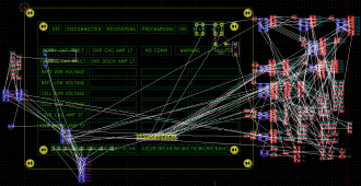
BTW today I did the layout (I didn't have the courage to put all the texts yet, especially since they are just placeholders) and started to place components:

HMIB_PCB_Layout.png
 
So both the Toshiba and the Infineon papers are wrong? I guess it's possible but very very unlikely IMHO.

Did I say they are wrong? No way. Let’s keep it real. I said Toshiba went through extra ordinary circumstances to get the fet to conduct.

You’re taking this scenario far beyond what Toshiba writes. According to you, all what’s necessary is a high dv/dt between drain and source with the gate connection open and the fet will conduct.

If the process of connecting battery power causes mosfets to conduct then this phenomenon would be extremely well documented.
 
Well, I'll do tests IRL when I have the MOSFET on hand and if I can't make them conduct then I'll remove that part of the circuit I guess.
 
  • Like
Reactions: Cal
Back
Top