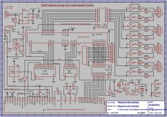
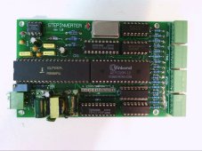
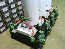
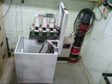
The scheme is similar to the original Trace inverter design but with batteries supplying the three sub-voltages directly.
This is using 9x12v =
108v, 3x12v =
36v, and 1x 12v =
12v.
Original Trace inverter uses
135v,
45v, and
15v.
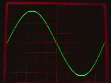
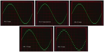
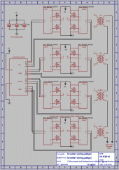
The H-bridges on each voltage level can produce +, -, or 0 voltage outputs.
Putting together the three voltages in series builds the pseudo sinewave, being a little choppy, with the discrete steps.
This gives 3^3 = 27 maximum possible discrete levels, although for regulation between battery voltage and AC output voltage the result is less levels being used much of the time. High battery voltage and low AC voltage gives the least steps with choppiest output waveform.
The Trace inverter used three transformers. I call them 'pappa bear' (135v), 'mama bear' (45v), and 'baby bear' (15v). Primary side of each transformer is driven by its own H-bridge from single battery (24v or 48v models). Secondary sides of transformers are just tied in series.
Since all series connected transformers' secondary sides have the same current, the 135v transformer supplies most of the power and is biggest transformer, the 15v transformer is the smallest.
Problem with this particular, direct from battery, transformer-less design is no isolation to AC output. Also, the charging of batteries in this transformer-less design cannot easily be done directly from the same path and would likely require three separate chargers.
View attachment 85572View attachment 85573


")