diy solar

diy solar

Cal's DIY BMS

That's a bit scary...

I recommend to log every variable you have before and after any calculation to see where exactly the problem is.

That's not normal and can lead to other problems even if you patch it here with a out of bounds check.
 
  • Like
Reactions: Cal
Just got done running a 17 hour test without accessing iPad WiFi. The data log has no voltage or current spikes. What's going on? Is this particular ESP32 defective or does everyone have a problem? I have another ESP32 to test. Do I need to halt calculations when WiFi communication is active? This is above my pay grade when looking inside the ESP32.

Temperature drop-outs are unrelated to WiFi as I've seen them before. I've added a -30C out-of-bounds evaluation and those spikes are now eliminated. :)
 
I never used an ESP32 so I can't answer that, but reading your posts I have less and less confidence in the ESP32...
 
  • Like
Reactions: Cal
I never used an ESP32 so I can't answer that, but reading your posts I have less and less confidence in the ESP32...
Your post turned the light on for me. It's not the ESP32, rather it's ME. No one else reports this problem, therefore it must be isolated to my setup. All 4 cell voltage calculations and the shunt current calculation have identical spikes. They always have the same spike magnitude. There's one thing in common with these calculations. They all have a thermal drift correction. Some how the wrong temperature enters the calculation, resulting in the spike. It's a bit perplexing since the temperature logged reading is correct when the spikes occur. I've added a temperature measurement reality check in my code. Since then the spikes have been eliminated. :cool:

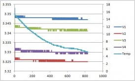
log4V.jpg

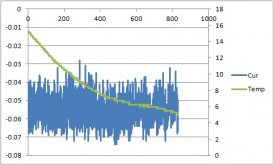
log4I.jpg

Temperature scale (deg.C) is to the right, with temperature going from 15C to 5C in 800 minutes. Data is recorded every 4 seconds. Current granularity is about 30 mA. I notice that the cell voltage thermal drift still needs some tweaking.

All is well again.
 
It's a bit perplexing since the temperature logged reading is correct when the spikes occur.
The mystery is solved as to why I'm not seeing a -126C temperature reading along with the voltage and current spikes. I'm logging data every 15th measurement. The previous temperature measurement was used to compensate for voltage and current thermal drift (not the current temperature measurement). After those calculations are completed a new temperature measurement is made. The code is now corrected so that temperature is measured first before voltage and current measurements/calculations are made.
 
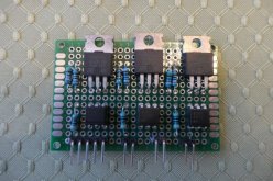
So far the circuit only monitors (and logs) cell voltages and load current. It's time to do some management! Here's the board I'm wiring up to do the under- and over-voltage disconnects. If I were to start from scratch, I would use an open collect configuration (actively pulling the relay coil to ground to energize the relay. However since I want this BMS to be a direct replacement for Chargery BMS, I need to build a high side switch (+12V energizes the relay).

The board has 3 sets of high side switches, consisting of a 4N35 opto isolator, and a P-Ch MOSFET. The third switch is used to trickle charge the motor home chassis battery. I had a very nice method to maintain a charge on the chassis battery. My charge controller has a secondary 1A output. Once the battery enters absorption and charging current begins to taper the secondary output becomes active, charging the chassis battery. Those were the old days when using a lead acid house battery. Now with LiFePO4 there's no absorption. Solar panel current is opened once over voltage is reached. Yesterday, after 3 months of storage the vehicle wouldn't start. I need a chassis battery trickle charger.

Chassis battery voltage will be monitored by the BMS. If voltage drops below 12.3V and house battery is above 13.3V then the chassis battery gets charged. I don't have a current limit resistor in place yet. I'm thinking of about 200 mA peak charge. The batteries will have about 1V difference in potential (13.3V vs. 12.3V). Current limit resistor would be 1V/0.2A = 5 ohms. Incidentally, there's 23 mA quiescent chassis battery current.

P1001609R.jpg

The 4 groups of connectors are:
3 ESP32 ports to activate the opto isolators and chassis battery voltage for adc measurement
Over voltage disconnect signal
Under voltage disconnect signal
Chassis battery voltage
 
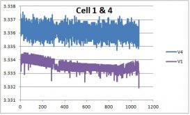
I'm about done with this design. Time to move on to new and improved. But first, I document some results. I have a 4-cell battery. Each cell has its own resistive voltage divider refenced to ground to enable a 2V referenced adc to safely measure the voltage. Measured voltages are (about): 3.3V, 6.6V, 9.9V and 13.2V. Cell 1 voltage is a direct measurement. But to get (for example) Cell 4 voltage, the 9.9V measurement must be subtracted from the 13.2V measurement. Due to the subtraction, Cell 4 ripple and measurement errors are twice as large as Cell 1.
Cell1_1&4.jpg

Neglecting the few spikes, Cell 1 ripple is about 0.7 mV. Cell 4 has perhaps 2 mV ripple.

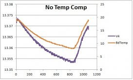
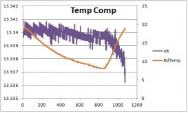
The circuit also has a huge thermal drift problem. Temperature in this plot goes from a maximum of 19C down to 8C. The measured voltage has a thermal drift of 20 mV. Not sure, I believe the internal to the adc voltage reference is the problem.
V4NoComp.jpg

Much of the thermal error can be compensated. Not sure why the voltage is dropping beginning at 900 minute mark. There's some ripple aliasing, perhaps caused by ADC1115 I2C communication?
V4Comp.jpg

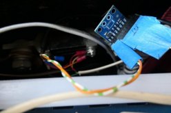
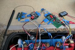
This is the entire circuit in operation. The BMS is capable of disabling loads or charging systems, monitor cell voltages, monitor vehicle chassis battery voltage, charge chassis battery (under specific conditions), measure shunt current, coulomb counter, measure cell and external temperatures, data log to SD memory, and send data via WiFi to my iPad. Looks like I need a packaging guru. Ha. Got to get some credit for matching the blue paper tape (which serves as wire-to-connector strain relief) with the blue 180AH CALB cells.
P1001618R.jpg

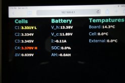
iPad data. V_h is the house battery while V_c is the chassis (starting) battery. All cell are at 3.333V. Cell 4 shows the largest error (3.370V). Time to move on to a new design.
P1001620R.jpg
 
On to the second generation cell voltage monitoring. I'm implementing almost an exact copy of BiduleOhm design. This is an improved design over the previous one. While the previous method measures two cell voltages (referenced to ground) and then subtracts the two adc values in the processor to arrive at a specific cell voltage, the new method does analog voltage subtraction before the adc converts the voltage to digital. The adc outputs the actual cell voltage, not a voltage referenced to a common ground.

I have a 100A and 300A shunt in the circuit. The 300A (low side) shunt measures the entire load, but will only be used when the microwave is in operation. The microwave pulls 160A. The 100A (high side) shunt records normal operation (7A max solar, 40A alternator dc/dc, 55A 120Vac converter, and max 10A loads).

I'll be purchasing parts from Mouser: MUX509, OPA2991, LTC2452, MPC1501-40, 100k ohm 0.1% 15ppm, 0.1 uF 50V. The resistor and cap are leaded parts.
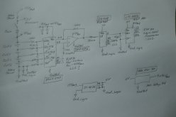
BMSsch1.0.jpg

Hand soldering this circuit together will be a major achievement. The 16-bit adc (LTC2452) for example is not much bigger than a flea!

LTC2452.jpg

This will get interesting.
 
The 330 Ohms resistor is maybe a bit small. You should check that the max output of the op-amp (basically around 14.5 V) limited by 330 Ohms don't go past the maximum current of the protection diodes of the DG408. I know 680 is ok with 12 V but not sure about 330 with 14.5 V. The ADC datasheet says that as long as your source impedance is less than 1 k the error introduced by that impedance will be less than 1 LSB ;)

If you only need one op-amp you can use the 991 (and if you need 3 or 4 you can use the 4991) ;) but IIRC the price difference isn't much and it's always nice to have a spare op-amp if you want to add features in the future, so yeah, do as you prefer ?

You might want to add some decoupling cap(s) right before the DC/DC converter as it might generate enough noise to be a problem (I guess you'll see during your tests).


Hand soldering this circuit together will be a major achievement.

Use drag soldering for the SMD chips ;)
 
  • Like
Reactions: Cal
Converted the schematic to a PDF file for easier reading. It's not a "real" schematic, but somewhat simplified to avoid too much detail. Some bypass caps are not shown. I'll check the 330 ohm resistor for adequate noise filtering. I just need one op amp right now. But it's good to have a spare.

Current measurement is not completed. I'll be using a INA 219 (12-bits) or 226 (16-bits) or 233 (16-bits) bi-directional current monitor. Will do some evaluations. The current monitor will be directly attached to the 300A and 100A current shunts. Communication is via I2C. That should be a simple, low noise design. The 100A shunt will be the main current sensor. Should current exceed 60A (microwave load) then current measurements will switch to the 300A shunt. Due to coulomb counting, I want to keep current measurements as accurate as possible.

Don't really need 16-bit resolution for cell voltage measurements, but these days it's hard to avoid them. What do you give up using 16 vs 12 bits? Conversion speed?

BMS schematic
 
I'll check the 330 ohm resistor for adequate noise filtering.

It's not for filtering but to avoid overloading the ADC input thanks to the protection diodes of the MUX.


Don't really need 16-bit resolution for cell voltage measurements, but these days it's hard to avoid them. What do you give up using 16 vs 12 bits? Conversion speed?

You gain speed with using less bits usually. That's why pretty much every scope is only 8 bits (and a few are 10 bits), they have very fast ADC so they can't be really precise at the same time.

You can search for a 12 bits ADC but note that given the input of the LTC2452 is differential you already have a 15 bits ADC instead of a 16 bits one... The difference in price isn't really worth going after a 12 bits ADC (especially since it'll probably be 11 ENOB at best...) but that's only my personal opinion of course ;)
 
  • Like
Reactions: Cal
It's not for filtering but to avoid overloading the ADC input thanks to the protection diodes of the MUX.

Yes, of course. The issue is, if op amp goes to positive rail (14V), the protection diode of the mux conducts. The DG408 absolute max input current is 30 mA.

330 ohms is just at the edge: I = (14 - 0.5 - 5)/330 = 26 mA

The OPA2991 has 75 mA max output current. So there's enough current to stress the mux. Why not add a small signal diode from mux IN to 5V to provide additional clamping protection?

I'm not sure if the 100 nF cap at the input to the adc is a good idea. Input resistance to adc is: 330 ohms plus 100 ohms (mux) = 430 ohms. The RC time constant is 43 micro seconds. Voltages may not be settled when switching the mux to another input when adc measurements are made. Perhaps 10 nF is a better choice, or smaller yet? Also, OPA2991 max load drive capacitance is 1 nF.
 
The OPA2991 has 75 mA max output current. So there's enough current to stress the mux. Why not add a small signal diode from mux IN to 5V to provide additional clamping protection?

Why not put a 470 Ohms resistor? You can add diodes (that's what I did with D241 actually, but that's because my voltage can go pretty high) but using a higher value resistor avoid the need to do that.


I'm not sure if the 100 nF cap at the input to the adc is a good idea. Input resistance to adc is: 330 ohms plus 100 ohms (mux) = 430 ohms. The RC time constant is 43 micro seconds. Voltages may not be settled when switching the mux to another input when adc measurements are made. Perhaps 10 nF is a better choice, or smaller yet? Also, OPA2991 max load drive capacitance is 1 nF.

Just add some delay in software. Also note that the 2452 starts a new conversion as soon as the data transfer ends.

Having the resistor in series isolate the op-amp from the capacitance (the 1 nF value is for a capacitor directly connected to the output), there's more info on page 28 of the datasheet about that. But you can put 10 nF if you want, the 100 nF value is mainly because I already have it in the BoM ;)
 
The order is in. Voltage ref MAX6070 is back ordered. Won't see parts till end of Feb. $50 order for 2 sets.

I'll increase the resistor size. Under normal conditions the op amp output shouldn't go to 13V. Perhaps if one of the cell voltage sense wires gets disconnected.
 
Ok ;)

Yep, I know in normal conditions it shouldn't happen but a BMS who destroy itself because you forgot to connect one of the balancing wires isn't a proper BMS to me ^^

Also the ADC is used for pretty much every measurement and it is kind of a PITA to change so I chose the option to protect it well enough so it never dies because of user error.
 
Started the shunt current measurement redesign. I'm using a INA226 and am very impressed with results. I'm getting 6 mA granularity using a 300A, 75 mV shunt.

P1001624R.jpg

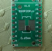
The INA266 is already soldered on a small module that can be purchased for a couple of bucks. The 300A shunt is located just to the lower left of the module. 4 wires go into the module: Vcc, gnd and I2C. Very simple. Initially I thought there would be a problem with the input filter. I absolutely need to filter the 120Hz current ripple when the microwave is on. The datasheet suggests max 10 ohms and 1 uF cap. That's only a 8 kHz filter. Far from what I want. What makes the INA226 very interesting is that there are:

a. 8 programmable adc conversion times from 140 us to 8.2 ms
b. 8 programmable adc average calculations from 1 to 1024

I chose a conversion time of 1.1 ms and 1024 averages. That means the adc outputs an average measurement every 1.12 seconds. There's just one I2C buss access to get an average of 1024 measurements. This duration encompasses over 140 120 Hz cycles. There's no need for a hardware filter.

INA226_1.jpg

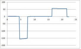
This chart shows -160A peak microwave load followed by 55A converter charging. Time in minutes.

INA226_2.jpg

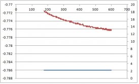
This chart shows -0.786 A quiescent current (blue line), and temperature (red curve) with temperature scale to the right. Temperature decreases from about 18C to 13C. Current measurement is rock solid. No thermal drift or noise. 1024 averages works well.
 
Got my parts from Mouser. This is the second generation bms.

P1001671R.jpg

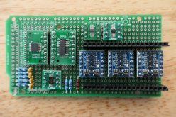
Bottom left are the 100K input resistors and 0.1uF filter caps. To the right is the difference op-amp, and two associated 100k resistors. Above the op-amp is the input multiplexer (MUX509) and a second multiplexer (DG408) that feeds the adc (LTC2452). To the right of the adc is the voltage reference (MAX6071). The ESP32 plugs into the black socket. Between the ESP32 socket are 3 sets of 4 bidirectional voltage level shifters that shift between 3.3V and 5V logic.

P1001672R.jpg

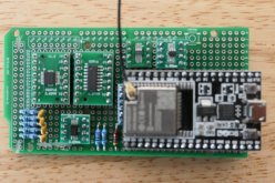
Seen here is the ESP32 attached. Still need to add some bypass caps. Nothing is wired up yet in the back. That may take me a week to complete.
 
You DIY BMS guys might be interested in this thread if you haven't seen it.

 
Powered up the 2nd gen bms today. I'm in troubleshooting mode. The analog section appears to work fine. But the LTC2452 (adc) doesn't respond. Connected the logic analyzer to the adc.

CS = channel 0
SCK = channel 1
SDO = channel 2
Should be getting data from SDO, but it remains low when SCK is toggled at 100 kHz. I sure hope the chip isn't dead.

LTC2452_CS.jpg
 
Are you sure you don't have anything that can keep the data line low? (mainly the MCU having that pin configured as an output)

Do you have an oscilloscope? (I don't really trust USB logic analyzers; especially if the signal isn't looking good)

Maybe try an idle high clock to see if it changes something.
 
  • Like
Reactions: Cal
Back
Top