diy solar

diy solar

Cal's DIY BMS

I don't think you should have those diodes on the input and output of your linear regulator. It should be ferrite beads on the input, if anything, and nothing in series with the output.

Also, use a real level-shifter and not one made manually out of fets.
Not sure what you mean. I have a small signal diode at the input to the linear regulator LM1117. The diode is for reverse voltage protection. I had already reverse voltage the circuit once, causing some of the chips to glow bright red! Yeah, I should be banned from touching any electronics.

One of the things considered is to use "real" level shifters. TI makes real low level shifters, not from 3.3V to 5V. There's some devices with open drains (SN74LVC1G07). They may work.

Regarding any errors caused by the resistor network to simulate cell voltages. The 390 ohm resistance is much smaller than the 100k input resistance to the opamp. I've also seen similar errors when connected to the real battery. The simulated cells are not the cause of the measurement error.

Edit, I now see you're talking about the diodes located in the JY-MCU module. That's not my design. The diodes are for protection. The module has a 3.3V output which I am not using. The diode connected to the 3.3V output is open circuit and a non-issue. I don't see the input diode to the linear regulator as an issue either.
 
Last edited:
Not sure what you mean. I have a small signal diode at the input to the linear regulator LM1117. The diode is for reverse voltage protection. I had already reverse voltage the circuit once, causing some of the chips to glow bright red! Yeah, I should be banned from touching any electronics.
Haha, that sounds bad. I actually meant the two of them in the level-shifter schematic with the yellow background. Those aren't needed. But yeah if you can't be trusted to hook up the voltage polarities correct, then you'd better include some protection for that! :)

TI makes real low level shifters, not from 3.3V to 5V.
Without looking, I'm 100% sure that TI makes a level shifter that works between 3.3V and 5.0V, as do many other chip companies. Now let me look one up for you. Here's the process to find it. First choose "Interface" products on their website.

https://www.ti.com/logic-circuit/vo...atch=LEVEL SHIFTER&tisearch=search-everything

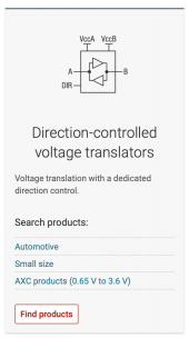
Since it's SPI you only need unidirectional translation, so click "Find products".
1620335330782.png
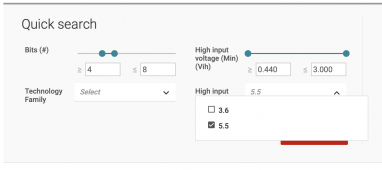
Set search parameters like this; you need at least 4 wires for SPI but let's not go crazy so 8 max:
1620335410984.png
And pick one with Vhi somewhere in the 0-3.3V range. 1.7V looks good. Only $0.39, too.
1620335476739.png
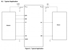
In fact the typical application diagram shows it being used for 3.3V/5.0V translation. See Figure 6 in datasheet:
1620335766716.png
 
  • Like
Reactions: Cal
The best level shifter is not using a level shifter. I do not think a fet level shifter can stand 100khz properly. That will depend on the mosfet the level shifter uses.
 
Last edited:
  • Like
Reactions: Cal
I do not think a fet level shifter can stand 100khz properly.
I think they can, actually. But yeah if you're having SPI issues that level shifter schematic is the first thing to toss out! The regulator shouldn't have those diodes, and you can just buy a part for the 4 bits that need level shifting. Much less wiring!
 
  • Like
Reactions: Cal
Regarding any errors caused by the resistor network to simulate cell voltages. The 390 ohm resistance is much smaller than the 100k input resistance to the opamp. I've also seen similar errors when connected to the real battery. The simulated cells are not the cause of the measurement error.
What it is clear is that there is a problem of non linearity in your measurements. Non linearity means that offset will depend on the level of the input instead of being constant.

The resistors can be small but the error is in the order of milivolts. The output impedance of a voltage divider is the top branch in parallel with the bottom branch.

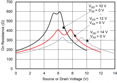
And that is added on top of the resistance and non linearity of the MUx.

1620336240435.png

That is why I suggested using buffers after the mux because you get rid of all these problems. If your mux and opamp datasheet recomends it, there is a reasion, not a conspiracy to order more opamps.

That opamp common mode rejection is high but the implementation kills it.
 
Last edited:
  • Like
Reactions: Cal
I also hope tolerance of the resistors is 1% (of the difference amplifier)
 
Last edited:
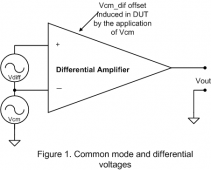
I just forgot to explain. Common mode rejection ratio (CMRR) is the ability to separate the common mode voltage from the differential voltage. Just to be an example.

1620338387155.png
Vdiff is the voltage of the cell we want to mesure and Vcm the other cells that are below. The idea is to separate Vcm from Vdiff using the difference amplifier. This capability is called common mode rejection ratio. If this capavility is low, offset will appear in the output proportional to the Vcm.

This depends on two things. One is the CMRR of the opamp and the other is the CMRR of the resistor network. Opamp is good (130db according to the datasheet) but resistor network..... your simulated cells have non-linear output impedance. Your mux also has non linear impedance. These resistances are included in the equation of the difference amplifier.

I hope resistor tolerance is at least 1% or better. It is not possible to have good CMRR in these conditions.

And this is four cells, with 16 where common mode voltages are highers, the problem is worse.

This can be calibrated by software but takes much much effort than just using the basic design rules.

There is toons of literature about this like for example:
 
  • Like
Reactions: Cal
My 100k resistors are 0.1%, 15 ppm.

BTW, TI selection guide didn't show the SN74LVCC3245 in the SPI application specific table. That's the source I was using for my search. It's a massive 24-pin part!

The goal is to measure cell voltage up to 4V. The ideal method is to use an unity gain diff opamp and a 4.096V adc reference. That means operating the adc from 5V. Unfortunately the ESP32 works on 3.2V. If we think the voltage level shifter is the problem then possible solutions are to either drop adc voltage to 3.3V or to use another level shifter. The current level shifter has no problem operating at 100 kHz. I believe I had it operational at 500 kHz. I also want to try a 200 ohm resistor at the adc SDO output. Speed isn't a issue. Just transferring 16 bits. I could drop clock below 100 kHz.
 
My 100k resistors are 0.1%, 15 ppm.
In my opinion it is a pitty to be in series with the resistance of the mux that can vary from 200ohm to 400ohm.

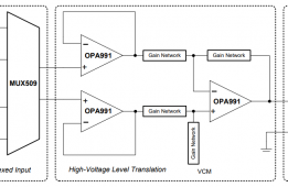
If you are just bored give a try yo assemble the circuit from the datasheet.
1620339649330.png
I think you will not regret.
 
  • Like
Reactions: Cal
In my opinion it is a pitty to be in series with the resistance of the mux that can vary from 200ohm to 400ohm.

If you are just bored give a try yo assemble the circuit from the datasheet.
View attachment 48052
I think you will not regret.
That's probably the next step and use a OPA4991. Not that much more effort. Adding some resistors to the mux inputs might be a good idea. This project won't be done any time soon. I got other activities going on in summer. But currently my main concern is why the adc is stressing out.

I don't think this is happening, but the opamp output has the capability to go to 13V. I added the clamping diode to help protect the adc. Should this diode conduct, the 5V rail will rise. The 5V linear regulator will back bias. It's possible the 5V rail rises above the maximum voltage of the adc.
 
One other tip, which you would have discovered looking at the SN74LVCC3245A more closely: you would need 2 of them for SPI since DIR is shared for all bits and you need 3 to go in one direction and 1 to go in the other.

For even simpler design, you could use an auto-sensing part like this 4-bit level shifter:
Propagation delays are approx 10ns or less, so that should be fine for 100kHz = 10,000ns SPI clock rate.

You may also be able to find the equivalent TI part, if you prefer to go with TI for some reason (like they're more generous in sampling free parts, usually!).
 
  • Like
Reactions: Cal
I remeasured the analog front end using the 390 ohm resistor network. The ESP32 is removed. Mux inputs are hard wired hi or lo to acquire a specific cell. I don't believe real battery measurements would be much different.

Cell1234
Cell Voltage3.2503.2433.2563.252
OpAmp Voltage3.2383.2083.3253.305
Delta Voltage /mV-12656053
 
One other tip, which you would have discovered looking at the SN74LVCC3245A more closely: you would need 2 of them for SPI since DIR is shared for all bits and you need 3 to go in one direction and 1 to go in the other.
The LTC2452 SPI requires just 3 lines: CS, SCK & SDO (2 in and one out). The SDO is the line that might be stressed.
 
I remeasured the analog front end using the 390 ohm resistor network. The ESP32 is removed. Mux inputs are hard wired hi or lo to acquire a specific cell. I don't believe real battery measurements would be much different.

Cell1234
Cell Voltage3.2503.2433.2563.252
OpAmp Voltage3.2383.2083.3253.305
Delta Voltage /mV-12656053
Well, I guess since this is the op-amp output and this doesn't yet involve the ADC, it must be a combination of error sources we discussed in that other thread:
- varying common-mode voltage causing a differential offset voltage in the op-amp
- resistor variation due to having separate input resistors for each cell
- resistor variation due to the mux series resistance varying vs mux input and vs common mode voltage

You could try just calibrating the offset (just subtract it digitally) and it may only change somewhat due to temperature and the common mode changes vs cell state-of-charge.

If you're interested in pursuing this architecture further you could consider:
- higher common-mode-rejection amplifier
- lower-offset amplifier (ie, a chopping amplifier)
- matched resistors, such as those integrated in silicon
- reducing current flow through the mux, so its resistance is less important
- an instrumentation amplifier or a fully-differential amplifier having the above

There are probably other solutions as well; I'll think about it tonight.
 
  • Like
Reactions: Cal
Without a whole lot of effort spent searching (literally just picked the lowest-offset amplifier in "Instrumentation Amplifiers" at Analog Devices and got lucky), what do you think about trying an ADA4254? It appears to be a transconductor-based low-offset front end, which is sort of state of the art (low offset transconductor-input instrumentation amplifiers were developed in the last 20 years, I think, unlike basic op-amps). It even has +/-60V input protection and 2 differential input paths so you could wire them up with the same voltage in opposite polarity and "chop" the signal. It includes programmable gain so you can maximize dynamic range in the ADC, and also reduce the effects of the ADC's offset. While you don't need to reduce this amplifier's own offset in all likelihood, chopping would let you cancel out the offset of the amplifier and the ADC by exercising both polarities of the differential output signal, and then averaging them digitally. Also, input impedance is ~infinite, so your mux resistance wouldn't matter like it does now.
 
Last edited by a moderator:
Some offset is to be expected and calibrated out in software, I never planned to have a super low offset with this circuit directly on the analog side, only low enough to be reasonable and removed with calibration ;)

Also, most of the offset comes from the common mode voltage, if you really want to lower it on the analog side you can use higher precision resistors (I planned 0.05 % ones) but just software calibration should be fine and give you a total error in the single digit mV across the LFP voltage range and across a 80 °C span temp range (and that's including the MUX too).
 
  • Like
Reactions: Cal
The BMS is functional again. Listed are two tables. The first table is data from previous cell voltage measurements using the resistor cell simulation. The second table is same measurements but connected to the real battery. I think we can conclude the resistor cell simulation has no, to very little effect on measurement accuracy.

Noteworthy, the adc readings are all just 1 mV off from the meter (UT61E+).

Resistor Cell1234
Cell Voltage3.2503.2433.2563.252
OpAmp Voltage3.2383.2083.3253.305
Delta Voltage /mV-12656053


Battery Cell1234
Cell Voltage3.2943.2923.2923.295
OpAmp Voltage3.2853.3603.3583.353
ADC output3.2843.3593.3573.352
Delta /mv-10676557
 
Last edited:
My apologies for getting Paul's name wrong. Ever since Peter, Paul and Mary...

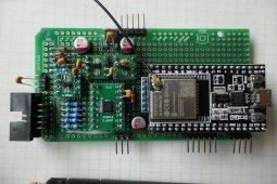
Just good news. BMS is close to completion. The adc LTC2452 is working great. As of yet, I see no need to average measurements. Cell voltage outputs are rock solid to 1 mV. WiFi is operational as well. Still need to do some thermal testing.

BMSgen3.jpg

There's 6 connectors. From bottom right:
1. Low and High Voltage Disconnect
2. SD memory card for data logging
3. Temperature sensor
4. Cell connections
5. 5V input to ESP32 (connected to 13V to 5V Buck regulator)
6. INA226

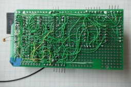
BMSgen3B.jpg

The back side looks ugly, but no way around it if it's hand wired.
 
Took some initial thermal tests. It appears cell voltage measurements have a negative temperature coefficient. As temperature decreases, voltage measurements increase. This test isn't completely accurate as the battery is loaded with the operational 75 mA of the bms. For further testing I'll use a lab supply to power the bms for more accurate results.

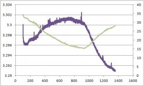
As temperature drops from 33C to 15.5C, cell 4 voltage increases from 3.296 V to 3.301 V, a difference of 5 mV. As temperature increases from 15.5C to 28C, cell 4 voltage decreases from 3.301 V to 3.291 V, a difference of 10 mV. Some of the cell voltage drop can be attributed to the 74 mA load. The bms consumed 1.5 AH over the measured time period

G3C4temp.jpg
Blue trace is Cell 4 voltage with scale to the left. Green trace is temperature in deg.C, with scale to the right. Time is in minutes. There is no averaging.

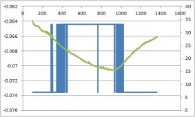
Temperature drift of the INA226 current is quite small. The 300A shunt has 9.2 mA granularity. Over the range 33 to 15.5C, current drifts by perhaps 9 mA. This deviation is most likely a thermal measurement error and not that the bms load current decreases with decreasing temperature.

G3CurTemp.jpg

The blue trace is current with scale to the left. Green trace is temperature with scale to the right. The measured current is quiescent bms current.
 
Back
Top