diy solar

diy solar

DIY BMS design and reflection

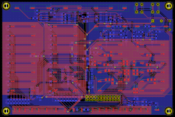
Tonight I finished the routing ?
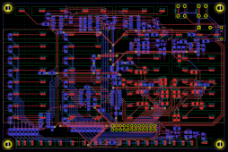
HMIB_PCB_Layout_no_planes.png


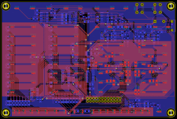
With the copper planes:

HMIB_PCB_Layout.png


I tried to keep the ground plane as clean as possible (the other planes are just power planes for the LEDs, they aren't critical at all) but I still had to stitch it in some places; here's the GND net highlighted:
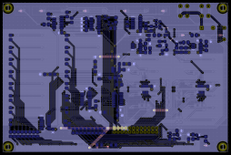
HMIB_PCB_Layout_gnd_highlight.png

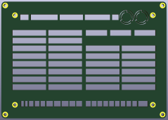
I have a few details to finish like the spacers and the front panel (they are basically empty PCBs with cutouts for the annunciators, etc...) and then it's done ?

The last board I have to make is the resistive balancer, after that I can make an order, then make and start testing the prototypes.


Sorry, no thread or site... Too busy on various project to accurately describe and update. I am sure you have spent quite some time on this forum. My BMS needs to be ready in two months... BTW I checked pricing and all silicon seems to have exploded. I have bunch of old ADS1211U's that are now over $35/pc?? Many items simply sold out with lead times >52 (!!!) weeks. Never knew you could speculate with integrated circuits, until now...

Yep, silicon shortage is a real PITA since months...
 
Tonight I've finished everything related to the HMI board ?

Final PCB layout:

HMIB_PCB_Layout.png


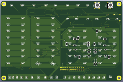
And some 3D views:

HMIB_PCB_Front.png

HMIB_PCB_Back.png


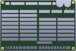
Then the spacer:

HMIB_Spacer_PCB_Layout.png

HMIB_Spacer_PCB_Front.png


And finally the front panel (and, yes, those flexures for the buttons were a real PITA to design because of the circular nature... and I'm not even sure they will be flexible enough, I'll wait to have a prototype to test that):

HMIB_Front_Panel_PCB_Layout.png

HMIB_Front_Panel_PCB_Front.png


So first comes the HMI board, then two spacers on top (probably 2.4 mm and 2 mm, but it depends on the exact height of the push-buttons; 4.3 mm in the datasheet...), then the front panel, and finally a translucent overlay with the texts and everything (probably made with vellum paper and self-adhesive transparent plastic to protect it).

Also, I checked and the MOSFETs aren't back in stock until august 2022 :rolleyes: and let's not talk about their price...

I decided to wait until I'm ready to order for the prototypes to sort this mess. I still have the balancing board to design first anyways.

Oh, also, Stephen (the guy designing a low cost PnP machine for DIYers) is basically done designing and testing it, and is now almost ready to make and sell kits, so that's really nice ?
 
This week-end I made the schematic for the RBB (resistive balancer board) and I also assigned the footprints so now I "just" need to route the PCB ?

I was able to halve the numbers of resistors by sharing them between two cells by using P-MOSFETs for half of the cells instead of N ones for all of them. I chose MOSFETs with a relatively high Rdson (around 80-100 mOhm) so they dissipate a small part of the energy instead of letting the resistors do all the work. The reverse polarity diode was selected for its Vf to dissipate part of total too. In the end the MOSFET will dissipate around 225 mW, the diode around 525 mW and the resistors around 5.25 W.

That's the total dissipated by the RBB at any given time but each cell circuit will actually dissipate half that on average since one cell can only be balanced at a 0.5 duty cycle at most, so the components should not get too hot given the generous margin on their power rating.
 

Attachments

  • BO_RBB_16.pdf
    154.7 KB · Views: 7
So... I advanced quite a lot tonight:

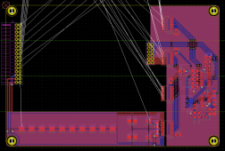
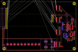
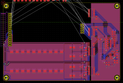
RBB_PCB_Layout.png

I know, I know... the copper zones are quite a retina burner... same without them:

RBB_PCB_Layout_no_planes.png


I almost finished one of the 4 power sections (the other 3 will be the same layout excepted for the one with the 12 pins connector which will be a bit compressed) but it's getting very late so I'll finish the few connections missing tomorrow. Here's more details of just the front side which is done (the other one is basically the same but mirrored on the X axis):

RBB_PCB_Layout_details.png

I'll try to find a 10 pins connector to replace the 12 pins one to have more room (I already moved it as much as I could without having the re-route half the BMSB...) as 2 pins have become useless after some design changes; but it is a bit special as it has long pins so it is both a male and a female connector so you can stack boards on top of each other.

If you wonder the resistors are 0612 ones which is the same as the classic 1206 package but with the solder sides along the length instead of the width. Here I use them mainly for the thermal advantage.
 
Last edited:
How many layers in the PCB? If more than two ...

Some I've designed had thick dielectric under top layer, but closely spaced planes inside.
I provided thermal vias down to an area of one plane, from which it was a thin dielectric away from full ground plane.
FR4 makes a pretty good thermal conductor with the right aspect ratio, and this spreads heat over entire area.
 
2 layers but if thermal is a problem I can always go to 4 and I can also try to mitigate some of it in software first if it's minor. I don't think it'll be a problem tho given the margin I have.
 
I was able to find a 10 pins connector to replace the 12 pins one and so I have much more room to fit the traces (especially since I need to maintain a 1.5 mm clearance between those traces and the connector because of the relatively high voltage difference) so that's nice ?

In addition to changing the connector and preparing the area around it, I also finished connecting the power traces to the first power section and I did another section:

RBB_PCB_Layout.png

RBB_PCB_Layout_no_planes.png

I was only able to copy-paste the copper zones (and even then I had to edit them one by one to change the net they were connected to...) everything else is done manually, so it's quite a time intensive process.
 
So far I've been using my DIY BMS without any balancing. I'm now looking to add this feature to my 4S 180 Ah battery. I like the concept of using 4 isolated dc/dc's connected to the entire pack, outputting 5V. Each 5V output is connected to a cell with a current limit resistor. Each dc/dc is activated via a fet when balancing is required. I thought of using just one isolated dc/dc and switching the output to the required cell. But that seems more complicated than just 4 dc/dc's. What do you think? Do you have suggestions for a dc/dc? Is charging the cell with 5V too risky?
 
It is more complicated but typically DC/DC converters are expensive, especially isolated ones. But since you only make one then I guess it's an acceptable solution if you're ready to accept the cost. But you still need to switch the converters off and on so you still need some level of complication...

I wouldn't use 5 V to charge a cell as I think it's too risky. I'd recommend either a 3.5-3.6 V or an adjustable converter, or at least a converter with a enable/disable input you control with something like a TL431 set to a safe voltage.
 
  • Like
Reactions: Cal
Consider a bidirectional or regenerative DC/DC converter, such as this:


Of course, at that point you're simply making a more complicated and expensive version of the existing active balancers on the market.
That's an interesting topology. But that's too complicated for my needs. There's no isolation either.

Using 4 buck dc/dc's, each with a fet for activation and regulation is simple and straight forward. Max dc/dc input voltage is 13.2V. My high voltage cell disconnect is set at 3.4V. That would result in a battery voltage of 13.6V exceeding dc/dc max rating. I could add a diode in series to knock down the input voltage.

Mouser sells these devices for $4. Any suggestions for a MOSFET that will turn on with a 3.3V signal? It needs to conduct about 85 mA max. Guess I could use a transistor to regulate the dc/dc. I have some of those on hand. They're perhaps 40 years old, but should work.
 
The ones I selected for my balancer have a super low Vgsth (like around 1 V IIRC) so 3.3 V isn't a problem, and they will be more than good enough for 85 mA ;)
 
  • Like
Reactions: Cal
I'm actually looking for a TO-xx package. Something with wire leads. Surface mount technology has made it extremely difficult to build one-of-a-kind breadboard. I'll stick with 2N2222A transistors.
 
Answering here to this post.

I don't have a prototype yet but I'll make sure to test it thoroughly once I do, including dead shorts with various amount of inductance.

From the datasheet each MOSFET can handle 1.0 kA for 10 µs and 1.1 kA for 5 µs (@ Tc = 100 °C) and there's 10 of them in // so the max is 10 kA for 10 µs. The short-circuit protection should have an end to end delay of a bit less than 3.3 µs and triggers at around 1 kA so that should leave plenty of margin even with a super low system inductance (I calculated it will be fine even with just the inter-cell busbars inductance), the peak current should stay far below the limit.

I'm more worried about the inductive kickback as I have less margin here than I'd want ideally, but real world tests will tell me if there's a problem or not anyway.
 
It would be nice if a BMS could periodically run an A/C signal through the battery to periodically determine the internal resistance of the cell. With IR cell reports, the monitoring could warn when a cell was mismatched or needed to be replaced before they become a danger. Also, knowing the IR of the cells in a string would allow the BMS to know the optimum charging parameters.
 
It will measure individual cell IR (not with AC tho since that would be too complicated and less accurate than a true DC IR measurement anyway) but only on user demand since it involves switching the loads on/off multiple times. In addition it will monitor busbar and balance leads connection resistance constantly during balancing (and it will also check the internal balancing circuit integrity too) and periodically when not balancing.

It will also track individual cell capacity (using the shunt and each cell voltage) so you can see outliers and to allow smarter balancing too (capacity based instead of voltage based).
 
I'm more worried about the inductive kickback as I have less margin here than I'd want ideally, but real world tests will tell me if there's a problem or not anyway.

Diode clamping, and maybe MOV?
MOV don't have tight regulation; has to be selected so some over-voltage could get through be applied but should clip extreme levels.

I suppose for tests you have to do long/short battery cables, large loops vs. tightly coupled.
 
Back
Top