diy solar

diy solar

I want to make my own BMS

It is not about the time, it is about the frequency of the situation.
Time is extremely important. What's the thermal time constant of a fet die? A few minutes? The battery might be subjected to below freezing temperature and hence charging is disabled. You would be utilizing the body diode for an extended time period. The fet can heat up quickly in this scenario. There are other cases where body diode current conduction duration is much longer than the thermal time constant of the die.

Let's do a simple design where the mosfet switch conducts 100A using your MOSFET. We'll use 3 fets in parallel, each fet conducting 33 A.

Power dissipation through fet:
P = 33A^2 * 2.7 milliOhm = 2.9W

Power dissipation through diode:
P = 33A * 1V = 33W

Do you understand that design won't work?
I really do not understand what you want to say but I do not have time to explain why it works. You should explain it to the hundreds of BMSs in the market using this design. Also to TI instruments and Linear technologies who spend hundred thousand euros designing chips to use this mosfet configuration. As I have said, I have not invented this. You can start checking the last link I published.

In the case that you are right, what solution do you propose for a 2 terms BMS with shared charging and discharging path?
 
Last edited:
Also have you checked the datasheet of the mosfet, the power it can dissipate and diagram3?
 
I really do not understand what you want to say but I do not have time to explain why it works.
Glad I am not the only one....


Do you understand that design won't work?
What does not work? The body diodes never really carry the load in a back-to-back MOSFET switch. I have this configuration in a lot of designs, it is not a novel concept at all. I learned it from app notes from TI, Linear, Fairchild, etc, etc.....
 
In diagram 3, taking into account Vds around 1V you can discover the maximum current the mosfet can handle when diode is used as explained in page 9 form the previous document. But it is much simpler than that. The datasheet says:

Captura.PNG

Always with the problem dissipation of course. In any case, drainning 100A under failure operation is not the plan.
 
With diagram 3, taking into account Vds around 1V you can discover the maximum current the mosfet can handle. This is explained in page 9 form the previous document. But it is much simpler than that. The datasheet says:

View attachment 33566

Always with the problem dissipation of course. In any case, drainning 100A during failure status is not the plan.
162A with an 800mV drop?
How do you avoid smashing Tjmax?

What am I even missing here.....at what point would the body diode be conducting?
 
That needs to be calculated with the final heatsing Rthja. I am just talking about what a mosfet can do technically. In any case it is not my point of discussion. That is something that will need to be calculated. I am also not planning to drawn 100A at 24v (2400W) or 48v (4800W) during failure. It is true that the dissipated power can be huge but in any case I am not planning to do this kind of discharges. The plan is only few amps.

What do you mean with what point? if you mean in wich situation I explained it in message #58. The plan is never. Just in case of failure to take some actions to mitigate the failure. And this is an extra feature that does not need to be enabled.
 
Last edited:
If you calculate the drop in normal operation at the rated 194A is 518mV.
 
If you calculate the drop in normal operation at the rated 194A is 518mV.
What's your point? That's not the problem.

The problem arises if you rely on the body diode to conduct full current during a over voltage or under voltage or temperature scenario.

At 33A, the diode will have a voltage drop of 1V. It will dissipate 33W. It won't be long before the fet is toast.

You're the circuit designer who wants to design a DIY BMS. Here's an excellent place to begin. Let's spec the current at 300A. How does the fet disconnect circuit look like?
 
But just for curiosity you just need to use the tools that datasheet gives. In order to disipate 163*0.9=147W (using the normal ON operation would be 102W) from 175 junction temperature to 25 ambient temperature (150 gradient) you need to guarantee 150/147= 1.02C/W dissipation.

Taking a look to the datasheet:
1610935227698.png

You need to guarantee a case to open air dissipation of 0.3 C/W to meet the max requieriment.
 
Can I ask again why we are talking about the body diode conducting any significant current for any time at all?

Perhaps I missed something
 
What's your point? That's not the problem.

The problem arises if you rely on the body diode to conduct full current during a over voltage or under voltage or temperature scenario.

At 33A, the diode will have a voltage drop of 1V. It will dissipate 33W. It won't be long before the fet is toast.

You're the circuit designer who wants to design a DIY BMS. Here's an excellent place to begin. Let's spec the current at 300A. How does the fet disconnect circuit look like?
Instead of stopping answering your answers I like to be honest. I am not going to answer this. I have already said many times that I am only planning to make flowing few amps through the body diode of the mosfets. I will never make flowing 300A through the body diode. During normal operation it is a different scenario.

I have already said planty of times how the circuit disconect looks like. I am not inventing it. As I have said it, this is the same as thousands of comercial devices and dedicated chips use. (If I say 100% of comercial devices using silicon based methods provably I would not fail)
 
Last edited:
Can I ask again why we are talking about the body diode conducting any significant current for any time at all?

Perhaps I missed something
That is the problem, I have never said I am planning to conduct a signigicant current. I have alsways said the opposite. I have always said that current requiered will be only the necesary to mitigate the failure, not to use the washing machine.
 
Last edited:
What's your point? That's not the problem.

The problem arises if you rely on the body diode to conduct full current during a over voltage or under voltage or temperature scenario.

At 33A, the diode will have a voltage drop of 1V. It will dissipate 33W. It won't be long before the fet is toast.

You're the circuit designer who wants to design a DIY BMS. Here's an excellent place to begin. Let's spec the current at 300A. How does the fet disconnect circuit look like?
I will ask again, in case you say my design is wrong, it is good to give an alternative, what do you propose for a BMS using shared wire for charging and discharging and not using mechanical relays?
 
Geeeez.....lets start over. Get out of the weeds and stop talking about the body diode.

Lets see a block diagram or something. Maybe some datasheets of parts being considered for various tasks. Anything except body diodes.

How will the cells be measured and monitored?
How will the system disconnect itself?
What methods are on the table for balancing?

Start with something higher level......
 
I will preper a high level diagram soon, also because I want to star dumping the information in a report.
 
What is your BMS going to do better or different than the rest of the pack?

Did you say its going to be on the positive leg?
 
There are few motivations for my project.
The first one is that price of Batrium is too high for the current cost of batteries.
The second one is that I need a BMS with low temperature cut-off. This is not easy to see in cheap ones.
A third motivation is the simplicity of the system. I want to implement telemetry. For this telemetry I need to add a shunt, and RPi and a rpi or something similar. Why not doing all of this directly from the BMS. Cheap BMS already offer telemetry but with their own applications are normally not good. I want to make a system that can send the measurements to cloud server, local server and remote server. I already worked in the past in a system to diagnose solar system using the data from them and performance over time.
A fourth motivation can be the flexibility of configurations. I would like to configure as I want. For example send an alert to my phone when temp is <7C, send an alert when batteries are charged.....
The last motivation is the capability of additional features like enabling heaters during low temperature events, active balancing, my own battery gauge algorithm..... whatever I can imagine as for example an algorithm to get the available power in the solar field when battery is full and use it for heaters or whatever (off-grid)

I just want a battery management system, not only a protection system.

Of course, features should be implemented and made them reliable in order of importance starting from protection.
 
Last edited:
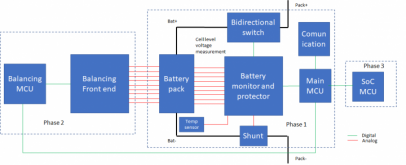
This is the block diagram I have planned, organized in phases of implementation
1610993171836.png
As phase 2 and 3 come later I prefer to star talking only about phase 1.
For the battery monitor and protecto I have thought about BQ76952. The highlights of this components are:
- 3 to 16 cells so it can be used in 12v, 24v or 48v systems.
- Voltage measurement. I don't need to use voltage dividers to measure with wil the MCU.
- Current measurement using a shunt. Same story.
- Temperature sensor input.
- Coulomb counting. Very useful for me as I do not need to do it manually in the MCU.
- LDO outputs to supply the rest of the devices.
- Voltage (high/low), current and temperature protection.
- Integrated charge pump to use high side n-mosfets as switch.
- Individual control of these n-mosfets for direction selection. (let's not discuss about this)
- I2C and spi comunication to configure the device and read voltage, current, temperature and coulomb counting.
- Passive balancing. I am not planning to use it but it is there.
- Unit Price: $3.68.

The advantadge of this component is that I can have all the protections done by hardware and avoid firmware bugs and so on. I think this chip is awesome for the cost.

For the MCU I am planning to go with a STM32 Cortex-M. I have not decided which one but all of the are the same. It only chages clock speed, memory, peripherals.....
The function of this MCU is to coordinate the whole BMS. In phase 1, it will read the measurements form the Battery monitor and transmit them. It will also receive new configurations from and reprogram the battery monitor.

For comunication I thing it is not necessary to be decided now. I could use Bluetooth, wifi.... whatever wired or wireless.

Something interesting I did in a previous project is having an USB input. Using a USB stick with a propperly formated TXT file with the configuration, you can connect it and reprogram it.

For the shunt I was planning using a shunt. Provably a 4 terms one for accuracy.

For the switch I will use an array of n-mosfets.

Another question you might ask is why 3 MCU in total. They are cheap, around $3 and it will provide bug and process isolation. In terms of complexity, STM32 are quite easy to work with, they only requiere few VDDs and ground and no external components. Only the comunication chip will need crystal so I can run then crystaless.

What do you think about this?
 
Last edited:
Back
Top