diy solar

diy solar

Laying out and ordering PCBs

Another interesting approach, since you are always measuring something with a large, fixed polarity (2.5V - 3.65V) would be to "subtract out" a reference voltage, allowing you to gain up the remaining difference and get higher signal before you saturate your ADC. Basically it would allow you to use your ADC's input range more fully by "zooming in" on the voltage range of interest, not wasting range on the first ~2.5V which is always present in LiFePO4 batteries.

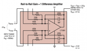
For example: you could do this using a part like this:

You'll notice it has 0.01% resistors, and a lot of them. If you hooked up your battery cell / mux output to two of those input resistors, and an appropriate reference voltage to two other input resistors, you could remove the "static" / "boring" part of the signal, and zoom in on deviation around a reference voltage (which may be 3.0V, for example).

Update: I looked at this a bit more closely and you would want to pick an amplifier like this with equal input resistors, since the battery cell voltages are centered around approximately 3.0V and that's also a common reference voltage. To use one like the LT1991 with its 3:1 resistor ratios, you would also want your battery voltage to reference voltage ratio to be 1:3 or 3:1. This isn't as common since then you would need a 9V or 1V reference voltage. It's doable; for example by dividing a 3V reference by three or multiplying up a 3V reference voltage by 3 but like I said originally, you'd have to choose an appropriate reference voltage. Unfortunately your original choice of ~4V reference doesn't have a very low lowest-common-factor with the 3V battery voltage, so that complicates the choice of resistors. To adjust the reference voltage just costs one additional low-offset op-amp.
 
Last edited by a moderator:
- OPA991 is reasonably low offset (125uV). You can definitely go lower-offset with a chopper amplifier, typically 10uV. In integrated solutions like inside the INAs, the chopping is synchronous to the ADC sampling. But, 125uV is probably ok for this application. More on this later.

Well, 0.13 mV offset on the cell voltages measurement is plenty good enough I think. Yes you can always use better op-amp, a better ADC, etc... but cost rise quickly for no real benefits. There's also other big constraints like the CMRR, having true rail-to-rail inputs and output, etc...


- The mux's resistance and the input resistors for each of its 8 paths will add to your gain error since it participates in the R2/R1 gain of the op-amp circuit. Ideally you would not have this source of error since it would use matched resistors on the opposite side of the mux. Assuming you stick with a discrete approach like this, you should at least move the resistors to the opposite side of the mux (which also eliminates the need for some of them). If you instead switch to the fully-differential topology I linked to above, the resistors are now integrated and matched for you inside the amplifier silicon, and you just have MUX -> DIFF_AMP -> ADC, fully differential the whole way, with no discrete resistors to worry about.

The MUX resistance mismatch is only around 0.0x % of a 100 k resistor, that's plenty good enough for cell voltage measurements. The idea with the resistors before the mux is that they are also a protection and limit the current in case of a user error in the wiring (although on a 4s system it's a smaller problem than on a 16s one) or if the MUX or op-amp decides to become a short for some reason.


- Similarly, you'll get better resistor matching if all 100k resistors are in a single package, as they are on a single integrated circuit, typically better than if you're using discrete 0.1% resistors like you did in your prototype design. The actual value is not important, only the matching is important.

I looked into matched networks but they are super expensive.


*Ok, a little expounding is in order: Right now you're relying on the input common mode rejection of the OPA991 which is a less optimal way to reject the varying common mode as you move up the stack of batteries with your MUX. You're also introducing a differential-mode to common-mode error at the ADC, since you're using a differential ADC in a single-ended mode. A reason to change it how I described above is because offset voltage and gain error are both common-mode-voltage dependent (in both the op-amp and the ADC). A second reason is that differential signaling is less susceptible to outside interference than single-ended signaling. On-chip stuff is fully-differential the whole way, typically.

I agree if it would be for the shunt but here it's for the cells voltages, it's plenty good enough and a lot better than any other BMS on the market in the same price range.

It's also because he used only a part of a circuit that is bigger and do more than just the cell voltages. He did that for the simplicity as it was already designed so it's probably not the best circuit ever for his appplication but it's plenty good enough and I don't think he wants to redesign the whole thing, but I can be wrong :)


Another interesting approach, since you are always measuring something with a large, fixed polarity (2.5V - 3.65V) would be to "subtract out" a reference voltage, allowing you to gain up the remaining difference and get higher signal before you saturate your ADC. Basically it would allow you to use your ADC's input range more fully by "zooming in" on the voltage range of interest, not wasting range on the first ~2.5V which is always present in LiFePO4 batteries.

That's a very interesting idea, but it would require a negative supply (I didn't thought about much more than 30 sec tho, there's maybe a solution without that).


Unfortunately your original choice of ~4V reference doesn't have a very low lowest-common-factor with the 3V battery voltage, so that complicates the choice of resistors. To adjust the reference voltage just costs one additional low-offset op-amp.

It's mainly due to being able to handle voltages up to 4.1 V, I also generate a 2.05 V ref from it which is used for various things and would be a bit more useful than the 4.1 V here I think.
 
Last edited:
  • Like
Reactions: Cal
You're giving off-the-shelf BMS too much credit. Chargery (BMS) current measurement couldn't be much worse. It neglects any charge or discharge current less than 1A. Current granularity is 250 mA for a 300A shunt. I know I can to better than that. Hence my project.

ah-over-25-hrs-jpg.23541


The chart shows after 17 hours, Chargery coulomb count is off by almost 15 AH! What the heck?

My BMS has a current granularity of 6 mA with a 300A shunt. A significant improvement over 250 mA! Yes, I can do lots better.
Yes! most commercial devices are ONLY considering the full power range.
I live here in a region where my solar harvesting is 95% at 5% irradiation and 5% at 75% irradiation. Both domains are providing ~ the same contribution.
So i have to cope with a lot of dynamic and the lower range must be performant.

Almost every commercial MPPT charger is a ridiculous underperformer in the lower 5% range if you use small panels.
 
Though I need to do more testing on my breadboard, I'm currently satisficed with the design. A design goal is to measure to 1 mV. With a 4.098V reference, adc granularity is 4.098/2^15 = 0.1 mV. Do we need to be better that? I don't believe so. What about the common mode errors? Are they so large that they affect the 1 mV goal?

I'm not sure about adding a filter capacitor across the feedback resistor. How much filtering are we looking for? To filter the inverter induced 60 Hz ripple? Or something above 100 kHz? I believe the voltage on the cap changes as the mux switches through the cells. There could be a significant capacitor voltage settling time when using a 60 Hz filter.
 
What about the common mode errors? Are they so large that they affect the 1 mV goal?

I calculated 2.4 mV typical and 8.2 mV max on mine but that's for 8s with 0.05 % resistors (and it includes everything in the chain, not just the op-amp, over the whole operating temp range). Actually 4s with 0.1 % resistors should be very similar. Also, most of it is calibrable, same as with any other offset and gain error. 1 mV should be do-able no problem ;)


I'm not sure about adding a filter capacitor across the feedback resistor.

I would carefully check first it'll not introduce a problem similar to the one caused by the capacitors that were after the 100 k resistors.
 
  • Like
Reactions: Cal
This is a great discussion we have going here! Thanks for reading it and commenting @BiduleOhm.

I looked into matched networks but they are super expensive.
They cost basically nothing actually. If you use an op-amp with integrated feedback resistors like the LT1991, those are already matched much better than discrete resistors. They are laid out in polysilicon right next to each other, fabricated in the same process just a few microns away from each other! They probably even use a common-centroid layout technique (Google that; it's fun to look at). Matched just means "very similar", it doesn't mean they're "trimmed" like with laser cut resistors. You're right that trimmed resistors are expensive but that's not what I'm suggesting.

That's a very interesting idea, but it would require a negative supply (I didn't thought about much more than 30 sec tho, there's maybe a solution without that).
No it would not require a negative supply. It's a differential circuit and you can connect +/-Vbat in one direction and -/+Vref in the other! I can draw it for you if you want, or you can just imagine "using another resistor pair" of the LT1991 diagram, with opposite polarity:
1618938024369.png

it's plenty good enough
Indeed, a lot of my comments are about making it better since he already has a good design. I thought the whole point of this exercise was to make something way better than an off-the-shelf BMS :).

The idea with the resistors before the mux is that they are also a protection and limit the current in case of a user error in the wiring (although on a 4s system it's a smaller problem than on a 16s one) or if the MUX or op-amp decides to become a short for some reason.
Yes, you're right about that. I thought of that after I typed my comments up but thought I'd gloss over that fact!

but cost rise quickly for no real benefits
I tend to disagree. For a hobby project you might spend $5 more on parts but then spend $100 for 8 boards when you only needed 1 board and $50 on shipping random stuff to your house. I don't think choosing better parts is a significant difference in cost for hobby projects. For real products, I agree. Also, there are real benefits...see below.
 
Last edited by a moderator:
I'm not sure about adding a filter capacitor across the feedback resistor. How much filtering are we looking for? To filter the inverter induced 60 Hz ripple? Or something above 100 kHz? I believe the voltage on the cap changes as the mux switches through the cells. There could be a significant capacitor voltage settling time when using a 60 Hz filter.
No, definitely not that low of frequency. Noise means thermal noise, not stuff like 60Hz interference which is too low to filter out with a practical filter bandwidth here. There is some higher frequency interference like ~10MHz from your microcontroller and the sigma-delta ADC which could be filtered out, were it to couple into the analog front end.

When you reduce the noise bandwidth going into the ADC you reduce the variation in your digital samples. It's basically just lowpass filtering.
 
I calculated 2.4 mV typical and 8.2 mV max on mine
I'd like to see that calculation. Or is it a measurement on your actual circuit?

Seems like that error is 2x-8x the desired accuracy of 1mV...so you should probably switch to fully differential.
 
To put some numbers to the "zooming in" example, let's say you use an ADR130 1V reference and the LT1991 I showed above. There may be better component choices, but just for the sake of an example. Let's say the 50k, 150k, 450k inputs are V1, V2, V3. Then:

Vout = 9*V1 + 3*V2 + V3
V1 = -1V reference (that doesn't mean below ground, just you connect it with a certain polarity, differentially)
V2 = Vbat = 2.4 to 3.65V (for LiFePO4)
V3 = open / not used
Vout = -1.8V to 1.95V, relative to the Vref that you supply.

The ADC you've used has +/-FS = +/-Vref / 2 = +/- 2.048V, so this uses (1.95 + 1.8)/4.096 = 92% of the ADC input range.
What you have now is a unity gain buffer, so you use (3.65 - 2.4)/4.096 = 31% of the ADC input range.

Not that it matters in this case since 16b ADCs have become commonplace, but you have 3x worse dynamic range than you could have. Basically we get 3x gain on the signal of interest, which is 9.5dB, nothing to scoff at!

Now, the really optimal solution would combine this "subtract a reference voltage" concept with the "fully differential" concept. That's what I would design if I was doing this from scratch and/or in silicon. The LT1991 is not fully differential so there would be some amount of common mode variation remaining like you have now.

Now I'm going to go spend 10 minutes checking my equations!...looks like it checks out. In this example you would connect the 2.048V you have available to the "Vref" pin in the LT1991 diagram above and also to the ADC (-) input, instead of grounding that pin. Then the two op-amp inputs would be:

Vplus = (3*Vbat + Vref)/13 = 0.7V to 1.0V vs battery charge
Vminus = Vplus when in feedback

And the op-amp output would be:
Vout = 13*Vplus - 9 = 3*Vbat - 9 + Vref = 0.25V to 4.0V vs battery voltage

And the ADC input would be:
-1.8V to 1.95V (differentially)

This shows the gain of 3x and that everything is within your 5V supply (no dual-polarity supplies needed).
 
Last edited by a moderator:
  • Like
Reactions: Cal
This is a great discussion we have going here! Thanks for reading it and commenting @BiduleOhm.

Yes, thanks ;)


They cost basically nothing actually. If you use an op-amp with integrated feedback resistors like the LT1991, those are already matched much better than discrete resistors. They are laid out in polysilicon right next to each other, fabricated in the same process just a few microns away from each other! Matched just means "very similar", it doesn't mean they're "trimmed" like with laser cut resistors. You're right that trimmed resistors expensive but that's not what I'm suggesting.

Oh ok, I see. The problem is that I would need multiple packages (unless they do biiiig networks...) so they would need to be trimmed ones. However for Cal it might work since its only for 4 cells.


No it would not require a negative supply. It's a differential circuit and you can connect +/-Vbat in one direction and -/+Vref in the other! I can draw it for you if you want.

Yep, I see it now ;) I need to handle very low voltages because I'm LTO compatible but if Cal wants to do it then why not, the only problem is to add an op-amp to generate the additional Vref, so it's probably not worth it. Resolution isn't really the biggest problem here, thermal drift is.


Indeed, a lot of my comments are about making it better since he already has a good design.

And it's always a good thing to have new ideas ;)


I thought the whole point of this exercise was to make something way better than an off-the-shelf BMS :).

Well, we're already at this point ^^. The problem with always wanting more perfs is when to stop (I already changed the op-amps 2 times because I found better ones for no too much more money), at some point the ROI gets pretty low and I think we're at this point given our accuracy requirements.


I tend to disagree. For a hobby project you might spend $5 more on parts but then spend $100 for 8 boards when you only needed 1 board and $50 on shipping random stuff to your house. I don't think choosing better parts is a significant difference in cost for hobby projects. For real products, I agree.

Yep, I'm probably biaised a bit on that since I plan to make a real product in the end even if it started as a personal project at first.


No, definitely not that low of frequency. Noise means thermal noise, not stuff like 60Hz interference which is too low to filter out with a practical filter bandwidth here. There is some higher frequency interference like ~10MHz from your microcontroller and the sigma-delta ADC which could be filtered out, were it to couple into the analog front end.

When you reduce the noise bandwidth going into the ADC you reduce the variation in your digital samples. It's basically just lowpass filtering.

There's already a LP filter (1 k / 100 nF) in front of the ADC. And there was also some LP filters in front of the MUX but I made a mistake thinking I could re-use the 100 k resistors to be part of a filter too and there was a little problem: https://diysolarforum.com/threads/cals-diy-bms.14055/page-5#post-235506


I'd like to see that calculation. Or is it a measurement on your actual circuit?

Seems like that error is 2x-8x the desired accuracy of 1mV...so you should probably switch to fully differential.

It's calculated using the datasheet values. I did the calculations on the calculator but fortunately I kept the intermediate numbers I used:

Accuracies for -30 to +50 °C with offset and gain errors calibrated at 20 °C:

ADC (125 µV/LSB, 63 µV/LSB after 4:1 oversampling)
typ: 0.325 mV (offset drift: 0.1 mV, gain drift: 0.1 mV, INL: 0.125 mV)
max: 0.45 mV (offset drift: 0.1 mV, gain drift: 0.1 mV, INL: 0.25 mV)

Vref
typ: 0.471 mV (drift: 0.327 mV, long-term: 0.143 mV)
max: 1.454 mV (drift: 1.311 mV, long-term: 0.143 mV)

OPA2991
typ: 1.589 mV (offset drift: 0.012 mV, Vcm change: 1.575 mV)
max: 6.312 mV (offset drift: 0.012 mV, Vcm change: 6.3 mV)

As you can see most of the error comes from the resistors tolerance with the common mode voltage. But you can avoid most of it with calibration (ideally at the nominal voltage of the cells, or even better if you can use a multi point table). And if you don't cycle the BMS from -30 to 50 °C during your measurements the error will be under 1 mV no problem.


Not that it matters in this case since 16b ADCs have become commonplace, but you have 3x worse dynamic range than you could have.

Yep, I know, but resolution is really not the limiting factor here, and I recover most of it anyway with simple 4:1 oversampling + averaging.


The LT1991 is not fully differential though so there would be some amount of common mode variation remaining like you have now.

The main problem of the LT1991 is that it doesn't have rail-to-rail inputs and the output is only rail +/- 40 mV, and it has a rather high Ib. There's probably other problems but just the rail-to-rail problem is enough to make it unusable here.
 
  • Like
Reactions: Cal
The main problem of the LT1991 is that it doesn't have rail-to-rail inputs and the output is only rail +/- 40 mV, and it has a rather high Ib. There's probably other problems but just the rail-to-rail problem is enough to make it unusable here.
It doesn't need rail to rail inputs. The inputs would only see 0.71V to 1.0V by my calculations! Also, it only gets within 250mV of the rails on the output, so +/-40mV is totally fine.

I don't think 100uA is "rather high" current consumption, but I guess everything's relative. Isn't your ESP32 going to be burning 100x that?

By the way, I updated above with some numeric examples.
 
Last edited by a moderator:
Oh ok, I see. The problem is that I would need multiple packages (unless they do biiiig networks...) so they would need to be trimmed ones. However for Cal it might work since its only for 4 cells.
No you wouldn't. If you trust your MUX to not "blow up" and short its various inputs together, then you don't need any input resistors, saving you BOM and board area. The only resistors you would need would be integrated in the op-amp package like I showed with the two parts I linked.
 
It doesn't need rail to rail inputs. The inputs would only see 0.71V to 1.0V by my calculations due to the magic of feedback! Also, it only gets within 250mV of the rails on the output, so +/-40mV is totally fine.

Ah yes, you're right ;)


I don't think 100uA is "rather high" current consumption, but I guess everything's relative. Isn't your ESP32 going to be burning 100x that?

I was talking about Ib, not Iq.


No you wouldn't. If you trust your MUX to not "blow up" and short its various inputs together, then you don't need any input resistors, saving you BOM and board area. The only resistors you would need would be integrated in the op-amp package like I showed with the two parts I linked.

I can't trust it for that, and I can even less trust the wiring to the cells to be correct.
 
OPA2991
typ: 1.589 mV (offset drift: 0.012 mV, Vcm change: 1.575 mV)
max: 6.312 mV (offset drift: 0.012 mV, Vcm change: 6.3 mV)
I assume you mean "Vos" change, not "Vcm". But for comparison, LT1991 is 1uV/degC max, so your 130degC * 12uV = 1.575mV, which is already 50% over the 1mV target @Cal wants. With the LT1991 it becomes 0.13mV, actually meeting the target. Or, maybe I'm misunderstanding where your calculation comes from in the TI datasheet.

Your point about input bias is interesting. I suppose 2.5nA * ~50k input resistance creates 125uV of voltage. But, that is common to both inputs, not differential. It's only if one input had a lot of leakage current and the other did not that it would make any difference in this circuit. It's likely just ESD devices leaking based on temperature so I'd say it's irrelevant here.

One other thing to note is that TI is a bit more liberal with their datasheet claims; maybe this is just my perspective from Analog Devices, but when TI reports max statistics they may only be 3 sigma and Analog Devices are 6 sigma. This is maybe just folklore though :).
 
Last edited by a moderator:
  • Like
Reactions: Cal
assume you mean "Vos" change, not "Vcm".

By Vcm I mean the input common voltage, not Vos. NB: this was only intented for me, I just copy-pasted it here, so notation may be not the clearest, etc.


But for comparison, LT1991 is 1uV/degC max, so your 130degC * 12uV = 1.575mV, which is already 50% over the 1mV target @Cal wants. With the LT1991 it becomes 0.13mV, actually meeting the target.

I have a 80 °C difference on the operating temp range (-30 to 50 °C).


One other thing to note is that TI is a bit more liberal with their datasheet claims; maybe this is just my perspective from Analog Devices, but when TI reports max statistics they may only be 3 sigma and Analog devices are 6 sigma. This is maybe just folklore though :).

Of course I plan on fully testing and checking with real measurements those numbers are correct ;)
 
  • Like
Reactions: Cal
Ah, I see.

Actually I think I made a mistake calculating the Vcm variation and included only the component which is attributed to the cell voltage, not the cell position in the stack. The schematic @Cal shared varies roughly by half the cell negative voltage, due to the 100k/100k divider. So the common mode varies by roughly 6.1V in a 14.6V battery as you cycle through MUX settings, going from top-of-bottom-cell to top-of-top-cell.

The one I posted would be:
Vplus ~= Vcm = (3*Vbat + Vref)/13
Vbat = 2.4V to 14.6V (top of bottom cell to top of top cell)
Vref = 2.048V
So Vplus would actually vary from (3 * 2.4V + Vref) / 13 to (3 * 14.6V + Vref)/13,
which is 0.711 to 3.52V

(Math edited)

So, it's not perfect but it is ~2x better. The fact that Vos is 12x lower in the LT1991 and the Vcm variation is ~2x lower combine to give you something with much better common-mode-induced-offset rejection. Specifically, it should be about 24x better! This is not even factoring in the improvement from better-matched resistors when they are integrated on silicon.
 
Last edited by a moderator:
Ah, I see.

Actually I think I made a mistake calculating the Vcm variation and included only the component which is attributed to the cell voltage, not the cell position in the stack. The schematic @Cal shared varies roughly by half the cell negative voltage, due to the 100k/100k divider. So the common mode varies by roughly 7.3V in a 14.6V battery as you cycle through MUX settings.

The one I posted would be:
Vplus ~= Vcm = (3*Vbat + Vref)/13
Vbat = 2.4V to 14.6V (top of bottom cell to top of top cell)
Vref = 2.048V
So Vplus would actually vary from (3 * 2.4V + Vref) / 13 to (3 * 14.6V + Vref)/13,
which is 0.711 to 3.52V

(Math edited)

So, it's not perfect but it is 2.6x better. The fact that Vos is 12x lower in the LT1991 and the Vcm variation is ~2.6x lower combine to give you something with much better common mode rejection. This is not even factoring in the improvement from better-matched resistors.

Well, maybe I'll use something like that in a next version then, but I can't redesign that part again or the BMS will never be finished ^^
 
Well, maybe I'll use something like that in a next version then, but I can't redesign that part again or the BMS will never be finished ^^
Lol, that's true here too, I have been top balancing for a week! I think my connections need tightening.

I also just edited that math like 10 times!
 
Hey @BiduleOhm check out these 0.1% 100k resistor packs (matched to ±0.025%, probably even better in all likelihood) and surface-mountable / pick-n-place compatible:


That's $0.43 per resistor in quantity of 1 package, which is more expensive than these 0.1% resistors in separate packages / non-matched:

0.01% go up to like $9 per resistor:
 
Last edited by a moderator:
It's very tempting but I checked and one network (I would need 2 + still need some of the single 100 k resistors for other things on the board) cost more than what all the 100 k (29x) cost on that board. Of course they are 0.05 % while those networks are twice better, but they would triple the total cost for the 100 k resistors.

My goal was single digit accuracy for cell voltages and I'm already here, even in the worst of worst cases. But I'll keep that ref on a corner of my notes as I'm sure it will be useful for a future version (maybe for the 8s one?), thanks a lot ;)
 
Back
Top