diy solar

diy solar

Taves BMS

Right now the system is collecting every 2 seconds. The cells are delivering the data in .4 secs for my 8s pack, so I can trivially go higher. Anything can be stuck into csv, so I don't see the point of that.
The point of storing the data into cvs is to graph it later. You may be collecting every 2 second, but it's not stored.

Good luck to you.
 
True, but on the other hand, it seems to me that a lot of the BMS choices are rather poor.

1) I don't see the point of BMS that has the circuits to deal with amps of the system. Just like we do not include an inverter or charger in the BMS circuit, which totally depend upon the amps, there's no point in putting the main cut-off circuit in there. Many of these BMSs have an ugly compromise between wiring sizing and physical mounting mass that suck. There should be a product that is both a shunt and a cut-off circuit, since this would combine 2 separate lumps of Amp related components into 1.
2) I don't see the point of a BMS that will only balance when at the top of the charge. These designs force a large heat sink, or no balancing capability onto the physical characteristics. It seems to me that people routinely equate balancing with some sort of requirement, instead of simply improving the capacity of the pack.
3) These BMSs are generally 12V or 24V and are not expandable with additional cell monitoring modules. I figure anyone that is buying a DIY setup, has a good chance of changing their mind in the future and adding some more cells, maybe in series. For example, the only reason I am not at 48V is because I can't find a reasonable 48/12V DC/DC converter that will deliver 70A @12V. The 48V choices are rather slim today, but I see no reason this won't change.
4) I don't have any patience with LCDs and pathetic UIs crammed into a few buttons. Any BMS that supports that will have a headache with customer support. I see no point to bluetooth either. WiFi allows you have a browser based UI that puts no restrictions on the buttons and UI. You can plug in just about any tablet or old phone if you want a dedicated UI mounted somewhere near the battery. There's no issue with security, except for ill-informed fear. The data can be sent to the cloud.

So, I am not limiting my thinking to just a hobby. Sure, the odds are that it will be just be a hobby, but I figure it makes sense to drive down costs which includes not only ICs on a particular PCB, but number of PCBs/enclosures. Right now, the product consists of 1 unit/product#/IPC that handles 12V, and 1 unit/product#/IPC that allows that to expand to 32s, supporting any Ns in between. The software, and thus user manuals and help, remain the same regardless of number of cells.

In addition I put plenty of thought into making a UI that is easy to use and won't F'up your batteries. I think about how the user will plug all this in and verify that they have wired it up correctly and set the settings correctly. There is a lot to do on that front.


I guess I meant that this is a lightweight conceptual discussion - which seem to be a fair enough assessment. Who knows where you would or could go with these ideas.

From the perspective of someone that has designed, engineered, built, tested, marketed, and sold all sort of products - you have roughly a million miles from here to there. That is not at all intended to be harsh, just a practical reality. If you have a pile of energy, you can make this a commercial product. I would guess that it would be very difficult to make a viable business in this market, but certainly not impossible.

A product like this has considerable liability, so consider the insurance and legal isolation required to deal with even one incident. Again, not impossible, but consider the effort and costs associated with a shark cage before jumping into shark infested waters.
 
I have taken some time to look at the various DIY BMS design efforts out there. In addition, I created some block diagrams and rough circuit designs of my own just for the learning exercise. Everything I have seen or come up with on my own is either complex analog design with a microcontroller only as a manager, or it is a fairly simple analog design with microcontroller as the primary control hub.

Neither of those approaches seemed interesting - too complex or too reliant on software.

After searching for some task dedicated silicon, I found the LT has some really nice parts where nearly all difficult tasks are all bundled together in a pair of packages.

LTC6811: Battery Monitor 16bit
https://www.analog.com/media/en/technical-documentation/data-sheets/LTC6811-1-6811-2.pdf

LT8584: Balanacing IC
https://www.analog.com/media/en/technical-documentation/data-sheets/8584fb.pdf

LTC3300: Active balance controller
https://www.analog.com/media/en/technical-documentation/data-sheets/LTC3300-2.pdf

These devices would allow me to design an extremely high-performance BMS in a few days. Done. Ready.
A microcontroller would be in the modest role of supervision, leaving plenty of options for current sense, dedicated coulomb counter, MOSFET high-current disconnect, etc, etc if needed. Integrated 16bit ADC directly coupled to the MUX. You will not design a more discrete system that approaches this performance. All the analog/ADC/processing happens on a single die.

The point being - I would almost certainly leverage the engineering expertise at Linear (now Analog Devices). The result is very high performance with a LOT LOT LOT less design effort required.

To be clear: By 'high-performance' I mean the functional electrical performance combined with very robust reliability.
 
The LTC6811 alone is almost 20 USD and only handle 12 cells.

And there's no current measurement with that solution.

I knew about those ICs but I wanted to avoid any specialised ICs (harder to source, super expensive, dependent on one model by one manufacturer) ;)


You will not design a more discrete system that approaches this performance.

I should have better performance than what I can see is the datasheet.
 
The LTC6811 alone is almost 20 USD and only handle 12 cells.
And there's no current measurement with that solution.
I knew about those ICs but I wanted to avoid any specialised ICs (harder to source, super expensive, dependent on one model by one manufacturer) ;)
I should have better performance than what I can see is the datasheet.

There is a balance between cost of the components and time to completion. That balance will certainly be different for everyone.
I suspect that you have many hundreds of hours into your design and have not yet laid out a PCB, which is another large project with all the analog. Then you have to gather all the more discrete parts, assemble a board and start with test and validatation to see what meets the expectations and what does not. This test phase can be more complex than the original design itself depending on how much you really want to know about the characteristics of the system. Depending on your own self-imposed specifications and quest for perfection - you will decided how many rounds of PCB design changes you can tolerate before calling the project DONE. From what I have seen of your project, I have no doubt the performance will be quite good.

Another approach is to leverage the many thousands of hours that go into the dedicated LT (and others) silicon devices and have a completed design that has very predicably high-performance at a small fraction of the design effort. Most of my design and manufacturing experience has been fairly specialized devises. The volume was usually rather low, so the cost of designing and prototyping was a bigger concern than optimizing the component cost.

In my personal scenario of a BMS product - I really just want a great performing and VERY robust power system that gives me control and status information. So far, I have not found that as a product which is why I have been engaged in these conversations.

I will trade high component cost for the option of drastically reducing design time and have a guaranteed result that meets or exceeds any of my expectations and needs. If I was making my own system, I would be done, manufactured, and out in the wild many many months or more ahead of anyone else.

As for current sensing.....I have been using a variety of devices but the INA226 is my most common device. TI just released the 'ultra-precision' 20bit 85v update all bundled up and ready to go. If integrated correctly, you can get nano volt and sub-millivolt precision for a few dollars. All the really hard parts have been baked into the tiny IC with full characterization data.

What is your time worth?
How many prototypes will you make before you call it done?
How many finished systems will you make?
What is the BOM cost (including assy) of each system?

Just a few questions that are always bouncing around my bench as I design things.
 
have roughly a million miles from here to there
Agreed
A product like this has considerable liability
True
I really just want a great performing and VERY robust power system that gives me control and status information.
Define "great performing and VERY robust". What does the solution I am providing not do that would lead you to a solution where you are spending $7 per cell instead of $1 (admittedly a very lame comparison because I am only pricing the main chip)?

The LT8585 will do active balancing, which is the ability to move current from one cell to the others instead of wasting it as heat. If you have solar panels and an off grid system, why do you care? You are throwing away way way more solar, because you have to have excess capacity.
Another approach is to leverage the many thousands of hours that go into the dedicated LT
So, why is the many thousands of hours that go into the dedicated LT better than the thousands of hours that go into the attiny?

Here is a load of nonsense from the LT8585 data sheet:

"This allows the weaker cells to continue to supply the load, extracting greater than 96% of entire stack capacity where passive balancing may only extract 80%."

I can assemble a set of cells where one is at 20% and another is at 100%, and plop on a typical passive balancing BMS that only drains power when the V is very near to the shut off V, thus it will take years to balance this setup. So why not advertise that passive balancing may only extract 20%?
 
Agreed

True

Define "great performing and VERY robust". What does the solution I am providing not do that would lead you to a solution where you are spending $7 per cell instead of $1 (admittedly a very lame comparison because I am only pricing the main chip)?

This a the question all engineers have to decide for themselves. Writing a specification that defines 'performance' is no small task. Writing a specification that defines 'robust' is even harder. That is partly why aerospace engineering is 90% paperwork. I have seen some spectacular failures of devices that were exposed to something the engineers 'didn't think would happen'.

In my experience - raw performance is relatively straight forward in most cases as it comes down to things you can directly measure. Voltage accuracy, clock jitter, power consumption, etc. Functional performance is where the raw performance metrics get combined to describe how well the device accomplishes it intended function. Raw automobile related performance being horsepower, torque, mechanical efficiency, or coefficient of drag. Functional performance being 0-60 time, top speed, etc.

The topic of 'robust' is more nebulous in general. That would describe how well the device will perform under non-ideal situations. How many single points of failure are there? Can it cope with balance leads being crossed? If someone keys a walkie-talkie right next to it - will it do something unexpected? What happens when the firmware locks up? Is the result of firmware locking up the same in every scenario? How many scenarios are there? How many corner cases are there that are out of the error handling range of the firmware?
....just some examples.


So, why is the many thousands of hours that go into the dedicated LT better than the thousands of hours that go into the attiny?

The ATTiny is a marvel of extremely versatile microcontroller technology. I have used them in a very broad array of devices and have nothing bad to say about them.

The problem is that any uC is a generic device that is not good at dealing with critical analog problems without a lot of external components and very good firmware. Being that ATTiny is only 8bits with very basic IO peripherals, its capabilities are very very modest in the context of power electronics control.

At a very minimum - I would have a separate watchdog uC or some analog components that catch glaring issues if the uC fails (usually a firmware fail). Analog UV/OV would be a good example to stop charge/discharge even if/when the ATTiny screws up.

In a design with the LT parts - you get very very robust design that has been put up against a myriad of very difficult scenarios and qualified by a team of experts using $multi-million lab full of amazing test equipment. All the uC does in that scenario is high-level monitoring and updating various registers. The critical responses are done inside the LT devices.

Is it worth the money? That is up to you. For me, I will gravitate toward the solution that has a guaranteed result, has the least likelihood of failure, and is simple enough that I could get it done before the world passes me by.

That last thing may be the most important. If it never gets done, none of its promises matter.
 
Here is a load of nonsense from the LT8585 data sheet:

Lol! The marketing department gets last looks before the datasheets are released. Marketing wankery can be good entertainment. Just look at the data.

Active balancing certainly has many advantages when money is no object and the end user wants every electron to come out of the battery. Off-grid and mobile solar systems don't really need that most of the time since they stay away from SOC extremes.

I am interested in active balancing for the pure experiment of how badly can my cells be mis-matched and still have a functional system. I think that the cost of a great active balancer could be offset easily by allowing the use of low-cost mismatched cells. Should be a fun experiment anyway.
 
There is a balance between cost of the components and time to completion. That balance will certainly be different for everyone.
I suspect that you have many hundreds of hours into your design and have not yet laid out a PCB, which is another large project with all the analog. Then you have to gather all the more discrete parts, assemble a board and start with test and validatation to see what meets the expectations and what does not. This test phase can be more complex than the original design itself depending on how much you really want to know about the characteristics of the system. Depending on your own self-imposed specifications and quest for perfection - you will decided how many rounds of PCB design changes you can tolerate before calling the project DONE. From what I have seen of your project, I have no doubt the performance will be quite good.

I'm definitely in the hundred of hours, but the 3 most complex PCB are fully routed (the two left to route are the one with the LEDs annunciators and the balancer, pretty easy boards ;) )

Given I made a lot of passes and corrected the problems I saw each time already, I should not have to make more than one revision (and ideally zero of course ^^) in addition to the first version.


Another approach is to leverage the many thousands of hours that go into the dedicated LT (and others) silicon devices and have a completed design that has very predicably high-performance at a small fraction of the design effort. Most of my design and manufacturing experience has been fairly specialized devises. The volume was usually rather low, so the cost of designing and prototyping was a bigger concern than optimizing the component cost.

Yep, I agree. The choice just depends on the priorities of each person of course ;)


I will trade high component cost for the option of drastically reducing design time and have a guaranteed result that meets or exceeds any of my expectations and needs. If I was making my own system, I would be done, manufactured, and out in the wild many many months or more ahead of anyone else.

And it's a valid method, but in my case it was just a personal project at the start, so time to manufacture wasn't really a problem ?


As for current sensing.....I have been using a variety of devices but the INA226 is my most common device. TI just released the 'ultra-precision' 20bit 85v update all bundled up and ready to go. If integrated correctly, you can get nano volt and sub-millivolt precision for a few dollars. All the really hard parts have been baked into the tiny IC with full characterization data.

Yep, I saw the INA and they seems pretty nice. I may use them in a future version (like a 4s or 8s version for example) ;)


What is your time worth?
How many prototypes will you make before you call it done?
How many finished systems will you make?
What is the BOM cost (including assy) of each system?

Just a few questions that are always bouncing around my bench as I design things.

Yep, I started to take all that into account when I saw some members were interested in fully assembled BMS.


The topic of 'robust' is more nebulous in general. That would describe how well the device will perform under non-ideal situations. How many single points of failure are there? Can it cope with balance leads being crossed? If someone keys a walkie-talkie right next to it - will it do something unexpected? What happens when the firmware locks up? Is the result of firmware locking up the same in every scenario? How many scenarios are there? How many corner cases are there that are out of the error handling range of the firmware?
....just some examples.

If you have time to write all the edge cases you can think of I'm very interested. I already planned against the most obvious ones (reverse polarity, swapping two balance leads, software locking up, etc...) but more is always better ;)


Lol! The marketing department gets last looks before the datasheets are released. Marketing wankery can be good entertainment. Just look at the data.

Yep, never rely on the marketing BS in the datasheets ^^ Promises in the text are BS, real data in the tables is what you're looking for ;)
 
If you have time to write all the edge cases you can think of I'm very interested. I already planned against the most obvious ones (reverse polarity, swapping two balance leads, software locking up, etc...) but more is always better ;)
I do not have the time to consider and analyze all the edge cases - which is what pushes me toward pre-considered silicon where all manner of insanity has been put on paper and tested before the massive cost of making a die and marketing a new device for many years. LT cannot afford mistakes so they cover a ton of edge cases on most devices.


And it's a valid method, but in my case it was just a personal project at the start, so time to manufacture wasn't really a problem ?

Since I have no plans to manufacture any of this - the restriction is that there is only so much free time available. In the context of these BMS concepts, I could have this thing done an prototyped in 40 hours and move on to the next fun project. Obviously differenent from my professional work, but a common theme - limited time.
 
It seems to me that there is a fixation on ADC accuracy that is not justified. I suspect this comes from several different sources. One is comparisons like "I am making one that is more accurate, therefore this other one is not accurate enough", and "this other chip delivers more bits, and it is easy to use, thus the other one is not good enough". Another is quoting specs from other BMS that, for example, only balance between a small range of voltage, thus they must have the accuracy to find that range. Many only will do cell draining when the cell is above some high threshold before the charger is cut off at the next slightly higher threshold. These are failing to properly comprehend the real use case of a solar powered off grid system, which is the market I am targeting.

The batteries are not sized so perfectly that you will be running them from 100% full to 0%. Thus why pick the 100% to 50% range, instead of the say 90% to 40% range?

If you are shutting off at N%, this means you are doing Amp counting and not using the V readings. Of course you must read the V on each cell because the Amp counting will drift. But notice that 3.5V is well within the exponential range, and 3.6V is totally acceptable, especially if you are only going there every few days or weeks when you suspect the Amp counting has drifted off. So if I had +-50mV accuracy, I would be fine if I set my cut off voltage at 3.5V. The only thing that the additional accuracy of say +-10mV gains me is more capacity.

It gains me more capacity for 2 reasons, 1) I can run the cells that much higher without worrying about frying the cell, and 2) I can get each cell up to that higher capacity. But note that the added capacity is not terribly important, because the difference between say 3.5V and 3.6V is jack squat compared to the excess capacity that you have bought.

I am sure that there are some installations where the battery pack is maxed out for their physical space in the RV and thus they really do want to routinely run from 100% to 0% and an additional 5% capacity matters, but those are rare. The majority of use cases is that they figured 150Ah was too small so they got the 280Ah battery.

There is a lot off emphasis on balancing the pack that all derives from lousy BMSs and a huge dose of being anal. There are several instances of fried batteries on this forum. My goal is to provide a solution where you can throw your batteries together, plop on the BMS and in a week or month depending on how far off they were, they will be reasonably balanced such that you have a reasonable % of the rated capacity at your disposal. I have no intention of risking the cells either on a bench balancing, or relentlessly running them up to 3.5V (or whatever your favorite cut off V is), for some anal achievement.
 
This a the question all engineers have to decide for themselves. Writing a specification that defines 'performance' is no small task. Writing a specification that defines 'robust' is even harder.
My goal of posting this thread was to get feedback on this specific topic. I apologize for being rude, but I wasn't really looking for general discussion regarding "performance" and "robust".

For me, I will gravitate toward the solution that has a guaranteed result, has the least likelihood of failure, and is simple enough that I could get it done before the world passes me by.

That last thing may be the most important. If it never gets done, none of its promises matter.
I am no expert on EE design, yet I made these and they are functioning right now. In other words, if I can design it and it functions, then it is probably pretty damn simple, no? I am measuring the V difference between the attiny readings and my digital multimeter at different temps today.

I can provide the gerber, BOM, and PnP files for ordering from JLCPCB.

Now that you've seen the circuits, do you have any helpful thoughts?
like a 4s or 8s version for example
You do understand that there's no 4s, 8s, or any other Ns version in my design, right?
 
I am bowing out of this thread.

Good luck and have fun.


My goal of posting this thread was to get feedback on this specific topic. I apologize for being rude, but I wasn't really looking for general discussion regarding "performance" and "robust".

If you have no interest in those concepts, I am scared of your product. That discussion was all about creating a reference point for you to be able to better understand where your design fits. That comes from decades of professional experience.....given to you for free.
I am no expert on EE design, yet I made these and they are functioning right now. In other words, if I can design it and it functions, then it is probably pretty damn simple, no? I am measuring the V difference between the attiny readings and my digital multimeter at different temps today.

Now that you've seen the circuits, do you have any helpful thoughts?

You can hack a lot of things together with an Arduino dev board. There is a reason that you find exactly ZERO arduinos in the power electronics industry.

On your circuits, I did not see the point in getting into details since my impression is that many of the core elements are poor choices. I like the concept of modular, I don't like how you are going about it. The schematics are a huge mess overall, but why bother addressing that when the majority of my suggestions are to re-consider bigger issues.

You can totally make a very basic BMS with what you have. It will satisfy some, but I would not trust it on my application for two reasons:
1. It is not robust.
2. The designer does not care about it being robust.

The ADC precision is about 10th on my list of concerns but I will spare you the details.
 
If you have no interest in those concepts, I am scared of your product. That discussion was all about creating a reference point for you to be able to better understand where your design fits. That comes from decades of professional experience.....given to you for free.
2. The designer does not care about it being robust.
Oh come on. Why do I get this response? I did not say I am uninterested in those concepts, nor did I suggest that. I asked for specifics! I asked how you define performance and robust for this functionality. That's exactly the opposite of uninterested, for goodness sakes.

I have reread your post three times now and I find no specifics that would enable one to judge what you require for your BMS.
In a design with the LT parts - you get very very robust design that has been put up against a myriad of very difficult scenarios and qualified by a team of experts using $multi-million lab full of amazing test equipment.
Except maybe this. Maybe you are saying that unless it is built with the LT parts, then it cannot meet your specs?
1. It is not robust.
Can you be specific?
 
This a the question all engineers have to decide for themselves. Writing a specification that defines 'performance' is no small task. Writing a specification that defines 'robust' is even harder. That is partly why aerospace engineering is 90% paperwork. I have seen some spectacular failures of devices that were exposed to something the engineers 'didn't think would happen'.

In my experience - raw performance is relatively straight forward in most cases as it comes down to things you can directly measure. Voltage accuracy, clock jitter, power consumption, etc. Functional performance is where the raw performance metrics get combined to describe how well the device accomplishes it intended function. Raw automobile related performance being horsepower, torque, mechanical efficiency, or coefficient of drag. Functional performance being 0-60 time, top speed, etc.

The topic of 'robust' is more nebulous in general. That would describe how well the device will perform under non-ideal situations. How many single points of failure are there? Can it cope with balance leads being crossed? If someone keys a walkie-talkie right next to it - will it do something unexpected? What happens when the firmware locks up? Is the result of firmware locking up the same in every scenario? How many scenarios are there? How many corner cases are there that are out of the error handling range of the firmware?
That comes from decades of professional experience.....given to you for free.
Just to be clear, this is free and just as valuable. All this does is attempt to define "performance" and "robust". It provides no BMS advice at all.
You can hack a lot of things together with an Arduino dev board.
This has nothing to do with an Arduino. I don't see the relevance.

Mine is running from a manufactured PCB board with only through hole items hand soldered. There are no cuts or jumps.
 
Last edited:
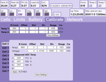
I implemented a handy way to measure the voltages and have the BMS record the ADC readings at that moment and save them. It will take up to 4 readings and do a linear fit to the data to determine the offset and multiplier to set the individual cells. You can see this UI below.

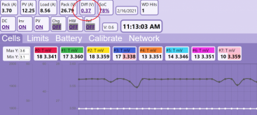
I found that the readings are within 15mv, or +- 7mv. Which seems acceptable. I have not tested over a wide range of temperatures though. Nothing prevents me from implementing a temperature coefficient. You can see below, that I have recorded the temperatures for the cells, but I don't do anything with that.

I have a noise problem that I need to solve. When my inverter is pulling 60A, the cell readings jump around. I suspect the noise is coming from the temp sensors, but I am not sure.

I have a design that includes a CAN bus ready to try, but I have no CAN bus devices.
Untitled.png
 
Back
Top