Monocrystalline technology was pioneered by Bell Labs , a wholly owned research arm of American Telephone and Telegraph Co. in the early 1950’s maybe patented in 1952. The very oldest solar cells were manufactured by Western Electric for use by AT&T communications repeater sites and for use in spacecraft.
Silicon cells did not do very well in space and gallium arsenide panels were favored for that enviroment.
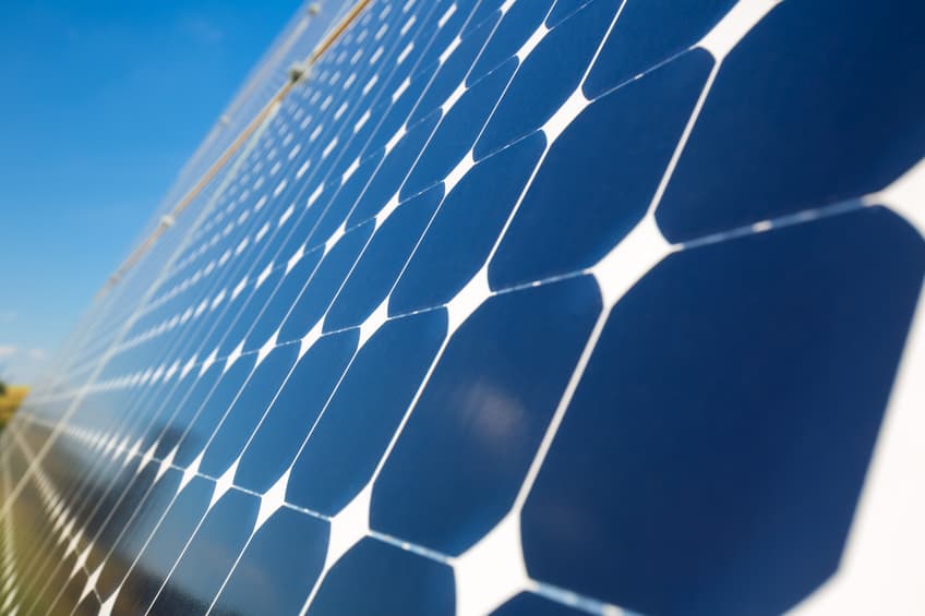
One of my engineering jobs was in Santa Clara, CA at a manufacturer of silicon ingots. These cells were grown in molten vats of silicon by lowering a “seed crystal” into the slowly rotating vat of molten semi-plastic silicon with the dopants already added in. The crystals were about 4” in diameter and about 30” long. After growing and a very long slow cooling process the ingots were machined round and then sliced into wafers. They were basically wafers for the production of 80486 processors wafers by Intel and other very high count semi-conductors on these wafers. The cells that were rejected for use in the semi-conductor industry were sold for use by solar panels manufacturers.
Polycrystalline technology came much later, maybe by 1979-1982 but is a very much simpler less expensive process.
I had never worked in that segment.
Most of my panels are polycrystalline but I do have several array’s of very much newer technology panels which are amorphous polysilicon over a monocrystalline base crystal jointly developed my Sanyo and Panasonic in a technology joint development project. Unlike other panels the voltage is markedly higher so integrating them is an issue. I‘m seeing 53.5 volts at MPP for the 96 cell panels which is too much of an offset from normal panels.
I also have a set of CdTe panels which have no cells at all, they are vapor deposited Cadmium Telluride on glass, 72 V.O.C. with maybe 154 separate segments on the panels, hard to see and count
And About 30 of the Siemens SM-55 which is the ARCO solar M-55 manufactured by Siemens just after Siemens bought Arco Solar