You are using an out of date browser. It may not display this or other websites correctly.
You should upgrade or use an alternative browser.
You should upgrade or use an alternative browser.
DIY BMS design and reflection
- Thread starter BiduleOhm
- Start date
Good question ?
The +5 V is generated from the +12 V rail (on another board) so the +12 V output of the main +/-12 V DC/DC converter is a lot more loaded than the -12 V output as a result. As the 12 V sent to the DPB is only used by the isolated DC/DC converters it doesn't matter if it's + or - 12 V with respect to ground and so I chose to use the -12 V rail to balance as much as possible the powers consumed on the + and - 12 V rails.
Now I checked the schematic and... of course I inverted the input polarity like an idiot ? Fortunately I didn't route the power supplies yet so I can easily change that. Good catch and thanks for telling me
Yep, exactly, I attached the corrected schematic 
In pure theory, no. But when the mosfets are turned off the floating ground would be only connected via capacitances and I don't like that (mainly because of EMI coupling into it) so I added a resistive path. It's probably not needed but it's only 2 resistors and they are less than a cent each so I prefer to be safe.
In pure theory, no. But when the mosfets are turned off the floating ground would be only connected via capacitances and I don't like that (mainly because of EMI coupling into it) so I added a resistive path. It's probably not needed but it's only 2 resistors and they are less than a cent each so I prefer to be safe.
Attachments
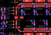
Today I advanced quite a bit on the routing :

This should be the definitive placement for the mosfets and their passives (I'll move the whole block to the left once the rest is routed). I have 26 mm at the top and bottom for 1" busbars on the front and 40-45 mm heatsinks on the back (so only 5-10 mm will protrude out of the board on the top and bottom).
In the middle I plan to have mini busbars (bare 2.5 mm² copper wire soldered); vertical ones on the front side for each pair of mosfets (Q150/160, Q151/161, ...), and a long horizontal one on the backside right in the middle to help equalize the currents in that part of the circuit.
Some details of the gates circuitry:

There will be zones ten times larger and on both sides, I just put the traces to remind me to be careful about how I route other traces in this area 
Also, it's part of the precharge and recover circuit so we are talking about a few dozens amps for a few seconds and a few amps continuous at most, it's not part of the 300 A circuitry.
Also, it's part of the precharge and recover circuit so we are talking about a few dozens amps for a few seconds and a few amps continuous at most, it's not part of the 300 A circuitry.
So... I've modified the schematic, again... but this time it's just to remove 2 resistors who weren't really needed. As always I attached the current version of the schematic.
Besides that I worked quite a bit on the routing:

I'm now sure everything can fit in 100x200 mm so that's nice ?
I had to battle quite a bit (and still haven't finished yet) with the routing of the mosfets gates circuitry for the precharge/recover circuit but I'm getting there...
Besides that I worked quite a bit on the routing:

I'm now sure everything can fit in 100x200 mm so that's nice ?
I had to battle quite a bit (and still haven't finished yet) with the routing of the mosfets gates circuitry for the precharge/recover circuit but I'm getting there...
Attachments
Guess what? I modified the schematic...  This time it was to add a 5th TVS as there was room and to change the temp sensors package from SOIC-8 to TO-92 as I had the idea to lay them on top of the first mosfet and bond them with thermal glue. I should be able to have a more accurate mosfet temp measurement that way.
I'm almost there on the routing:

I need to add a few traces for the temp sensors and then I'll be able to move the mosfet block to the left. After that there's only the high current zones to add and lots of vias (thermal and for current spread), like thousands of vias...
I'm almost there on the routing:

I need to add a few traces for the temp sensors and then I'll be able to move the mosfet block to the left. After that there's only the high current zones to add and lots of vias (thermal and for current spread), like thousands of vias...
Attachments
Ok, last schematic modification this time... Just removed a 100 nF cap who didn't make sense anymore.
I finished placing everything and routing almost all the traces (there's still a few short ones on the mosfets gates circuitry to route, easy but repetitive...), I also started putting the high current zones (and I already made a mistake, fortunately a small one: I need to cut the top right corner of the 2 small zones to leave more room for the B- connection bolt):

I finished placing everything and routing almost all the traces (there's still a few short ones on the mosfets gates circuitry to route, easy but repetitive...), I also started putting the high current zones (and I already made a mistake, fortunately a small one: I need to cut the top right corner of the 2 small zones to leave more room for the B- connection bolt):

Attachments
I'm improving as today I didn't modify the schematic... ?
I finished routing everything, putting all the high current zones and the vias for the secondary circuits. I still have to add the vias for the main mosfets and the holes for the B-/P- bolts (M8) and for smaller ones (M3 or M4) sandwiching the PCB between the busbars and heatsinks:

I finished routing everything, putting all the high current zones and the vias for the secondary circuits. I still have to add the vias for the main mosfets and the holes for the B-/P- bolts (M8) and for smaller ones (M3 or M4) sandwiching the PCB between the busbars and heatsinks:

So I've not done a lot today but I was able to add the bolt holes:

And to do that I added the busbars outlines first (in green):

They are perfectly identical excepted one has a corner cut; the dashed line is just to represent the center line, it was useful while designing. They are 25 x 135 mm (1" x 5 5/16"), the connection holes are M8 (5/16") sized and the other holes are M3 sized.

And to do that I added the busbars outlines first (in green):

They are perfectly identical excepted one has a corner cut; the dashed line is just to represent the center line, it was useful while designing. They are 25 x 135 mm (1" x 5 5/16"), the connection holes are M8 (5/16") sized and the other holes are M3 sized.
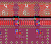
So... I added some vias... 197 per mosfet just on the drain side, with 159 of them just under the pad (I calculated I'd need a minimum of 120-130 vias to be thermally ok).
I've read a lot of articles (40+...) as I needed to have more solid info on thermal vias and the two I found most useful are those ones: https://www.ecomal.com/fileadmin/Da...rmal-Design-Guide-Enhancement-Mode-031815.pdf and https://www.ti.com/lit/an/snva419c/snva419c.pdf for those interested.
I also put the vias on the source and gate side to reduce impedance on the gate circuitry and spread the current on the source net.

Some details (those are 0.60/0.32 mm vias with a ~0.65 mm pitch in the center, a ~0.85 mm pitch on the rest of the pad and a ~1.25 mm pitch around the pad):

I still need to do some via stitching on the big zones for spreading the currents but the hardest work is done ?
I don't have one besides the schematic but I can do one. I can't do it now (it's very late and I'm exhausted after doing pretty much only vias placement for the last 7 hours...) and I'm not home this week-end but I'll do it as soon as I can
I've read a lot of articles (40+...) as I needed to have more solid info on thermal vias and the two I found most useful are those ones: https://www.ecomal.com/fileadmin/Da...rmal-Design-Guide-Enhancement-Mode-031815.pdf and https://www.ti.com/lit/an/snva419c/snva419c.pdf for those interested.
I also put the vias on the source and gate side to reduce impedance on the gate circuitry and spread the current on the source net.

Some details (those are 0.60/0.32 mm vias with a ~0.65 mm pitch in the center, a ~0.85 mm pitch on the rest of the pad and a ~1.25 mm pitch around the pad):

I still need to do some via stitching on the big zones for spreading the currents but the hardest work is done ?
It’s hard for me to get a full picture of your design. Is it possible for you to post a block diagram. It will be easier to see how everything fits together.
Thanks.
I don't have one besides the schematic but I can do one. I can't do it now (it's very late and I'm exhausted after doing pretty much only vias placement for the last 7 hours...) and I'm not home this week-end but I'll do it as soon as I can
Last edited:
There's no busbar and heatsink when soldering so it's not that bad as you always preheat the PCB before any soldering work anyway (especially on boards this big) to avoid warping it (and having problems with moisture exploding packages if there's already components on it). Also you can't really do better (if you can then please explain, I'd really love to know  ), thermal management is a higher priority than soldering. My biggest concern is actually the vias wicking the solder too much but I'll see if I really need plugged vias (more expensive...) or not, it should be ok with normal vias tho.
For DIY assembly I plan to preheat in an oven to 120-130 °C, and if there's enough interest and so I have boards assembled by a manufacturer then they'll probably use IR ovens and will just need to adjust the temp curve for it, they are used to that kind of stuff and have the right equipment.
@Cal I made the block diagram for the DPB: https://pastebin.com/T7CWRabx
I figured you had already thought about that. I felt compelled to comment because I've been there without an oven trying to replace components on a ground or power plane.
Many people have not, so it was a public service for those who don't understand the complexities of laying down parts on thermally engineered PWBs.
Many people have not, so it was a public service for those who don't understand the complexities of laying down parts on thermally engineered PWBs.
Trying to understand the gate drive. You have two sets of 10 parallel fets. Shouldn’t the two sets have separate drive circuits. Right now you have the two driver outputs connected together, going to all 20 fets.
Have you done an analysis that driver current of 6A is adequate to turn on 10 fets?
Do you know the thermal resistance of circuit board to ambient for the power fets?
One of the reasons I choose the Chargery BMS is that it doesn’t have fet disconnects. I don’t want a 200A fet disconnect. I can disconnect the Inverter with a low current command.
Many people have not, so it was a public service for those who don't understand the complexities of laying down parts on thermally engineered PWBs.
Yea of course
There's a lot of thinking about a lot of things you don't realize just reading this thread if you've never done that kind of stuff before. You need to think about your constraints but also some other things like larger scale manufacturing because if you use supra custom parts or a million assembly steps then it'll not scale well... For example I've done everything to avoid the cut corner on the busbar but I couldn't (well, I could but it would mean a longer PCB just for that... compromises...).
And that's not even an aluminium core PCB, you can go really deep really quickly in the rabbit hole ^^
Trying to understand the gate drive. You have two sets of 10 parallel fets. Shouldn’t the two sets have separate drive circuits. Right now you have the two driver outputs connected together, going to all 20 fets.
Have you done an analysis that driver current of 6A is adequate to turn on 10 fets?
So the design is maybe a bit unusual for two reasons: having enough gate current and redundancy.
The problem isn't really turning on the mosfets, it can take hundreds of µs I don't really care, it's turning them off fast. The faster I turn them off and the less the current has time to rise in case of a short circuit and that means less energy stored in the inductances of the circuit (mainly wires inductance) so less energy to dissipate.
The actual turn-off time just for the FETs is a hair less then 300 ns worst case and once you add the various delays of the full chain it comes to a bit less than 4.5 µs worst case. But I'll actually replace the op-amp for the current sense because I want more accuracy and so I'll try to find a faster op-amp while I'm at it, I may be able to shave 1 µs of the total.
So I needed two drivers to have enough gate current to turn them off fast enough. And then I saw that by connecting the two drivers outputs together I could add redundancy at the cost of only a trace and a few more resistors (bad idea to connect the outputs directly and also bad idea to not have one resistor per gate). And it has the side benefit of ensuring all the mosfets turn on and off at the same time, otherwise one half could be delayed relative to the other.
Do you know the thermal resistance of circuit board to ambient for the power fets?
I could do a simulation or calculations but I was more interested in the thermal resistance with a heatsink on the back (BTW much harder to find papers about that than for just a PCB to ambient). The PCB should add less than 4 °C/W which is low enough as I have 2.2 W worst case to dissipate per mosfet at 300 A so the PCB will add less than about 10 °C to the Tj at that power level.
I want to be able to handle 50 °C ambient, ideally 55 °C. I'll will see what heatsink size I really need after doing some real life tests. I designed with some margin at each step so I should be able to have pretty small heatsinks (still need to do the their outlines like for the busbars now I think about it...), with any luck they'll not even go past the board. I could also derate a bit like for example 300 A at 30 °C, 280 at 40 °C and 260 at 50 °C but I don't want to do that.
One of the reasons I choose the Chargery BMS is that it doesn’t have fet disconnects. I don’t want a 200A fet disconnect. I can disconnect the Inverter with a low current command.
Well, I don't trust whatever shutdown electronic they use in the inverter as it hasn't been made for emergency shutt-off but ony for a remote on/off switch. Also, doing that only protects against the inverter over-discharging the battery, it doesn't protects agaisnt anything else like short-circuits and it doesn't shut off the others loads. But all that is a personal choice of course
The on/off switch on my inverter is connected by a ribbon cable. That means on/off operation is controlled by milli amps. Insert a small relay in series with this switch and you got a rock solid disconnect for the inverter. After the inverter is taken care off the max currents might be in the 20 A range. A simple low cost fet disconnect works well here.
Shorts are taken care of by the fuse next to the battery.
Shorts are taken care of by the fuse next to the battery.
Similar threads
- Replies
- 8
- Views
- 372
- Replies
- 42
- Views
- 1K
- Replies
- 12
- Views
- 333
- Replies
- 0
- Views
- 81
- Replies
- 11
- Views
- 263


