diy solar

diy solar

DIY BMS design and reflection

So today I didn't work on the PCB but I made a spreadsheet for the power supplies to see if I was still within the DC/DC and linear regulators specs (I am, no problem) and to see the total power consumption so far (2.46 W but that's absolute worst case, typically it should be less than 2 W) :)

All cells in bold are calculated, the non-bold ones are data typed by hand.

Edit: corrected a small mistake in the linear regs values.
 

Attachments

  • Power.pdf
    34 KB · Views: 5
Last edited:
I didn't have time to do a lot today but I researched about what mosfets I'll use for the disconnect ?

The best (including cost/perfs ratio) one I was able to find is this one: https://www.mouser.fr/ProductDetail/ON-Semiconductor-Fairchild/FDBL86361-F085?qs=sGAEpiMZZMshyDBzk1/Wi/D7Em5shE8q79oNeZh9OawirCDuGpIRaw==

For thermal reasons I'd need 6 to 8 mosfets (depends on the heatsinking which is dependent on a lot of things; need to do real world testing for this one) per side as I want bidirectional capability (so total = 2 times that).

Then the question is about the short-circuit current I want to be able to handle. This mosfet can handle almost exactly 1 kA for 10 µs (for Tc = 100 °C, it can handle 1.4 kA at Tc = 25 °C but 25 °C is not realistic...) and unfortunately the curve doesn't go below 10 µs but looks like it's mostly linear in this region with a slope af about 30 A/µs. So for example for 5 µs (probably around what we can expect worst-case for the actual BMS design) it would be 1400 + (5 * 30) = 1450 but we need to apply the temp derating: 1450 * 0.707 = 1096 or a hair less than 1.1 kA.

So if we take the 14 kA example of a few pages earlier we need 13 (26 total) mosfets. At a bit more than 3 USD/each that is about 80 USD for the 26 mosfets. I don't know what you think about that but that's a bit too much for me. I guess I'll lower the short-circuit rating to 10-11 kA to have only 2x 9 or 10 mosfets (55-60 USD).

On the other hand I don't even know what the short circuit current will be because I don't have the cells yet so I can't measure the real DC internal resistance (the 14 kA figure was based on the AC measured internal resistance in the datasheet of the cell + some realistic length of wire), I have a slight hope it'll be lower than my estimation so I can use less mosfets...

If someone thinks he can find a better (lower cost/perfs ratio for at least the same perfs) mosfet for the task (Bvdss: 70 V min, 80 V or more preferred; Vgs: +/- 10 V min, +/- 15 V or more preferred; Rdson: don't care as long as the total dissipation of the whole disconnect at 300 A is less than 30-35 W; don't care about the package: can be SMD, TH, ...) he is very welcome ?

BTW: based on these results it's interesting to see that a classic ready-made BMS stands [almost] no chance to survive a short-circuit as it'll use far less robust mosfets (and probably not from a top tier manufacturer either) and rely on software (very slow compared to hardware) to detect an over current situation.
 
I have feared since the beginning of this thread that the mosfets would be a significant portion of the manufacturing budget. Would active balancing change the design parameters of the mosfets in a more cost effective manner?
 
I have feared since the beginning of this thread that the mosfets would be a significant portion of the manufacturing budget.

Oh I knew that too, just didn't know exactly what to expect exactly until now. It's actually not too bad if we don't care about the short-circuit handling capability.

Would active balancing change the design parameters of the mosfets in a more cost effective manner?

How so?
 
Ah ok. The only thing I was able to think of to lower the cost this way was economy of scale but using these mosfets for balancing is super overkill :)
 
Also, the interesting consequence would be the BMS turning into a lava blob in those 10 sec... ?

More seriously, I searched more about the mosfets, including on other sellers websites like Digikey and Farnell and the FDBL86361-F085 is still the best compromise I can find so that's what I'll use.

Now I have an interesting idea about mechanical design for the heatsinking and high current connections but it would mean the heatsinks are electrically connected to the mosfets drains so you'd have at least 2 heatsinks, one connected to B- and the other one to P-. So you can't let anything electrically connected to something touch the heatsinks, or connect them together. It's not a problem for me but I'm not sure for everyone else. I know it's a downside but apart from that there's a lot of advantages, especially about the thermal and high current path aspects. What do you think?
 
Last edited:
Yep, that's what I thought ;)

So driving the mosfets will be a fun thing on its own too as each one has a bit less than 13 nF of gate capacitance, for 20 mosfets we're talking almost 260 nF... but the current needed shouldn't be super high either as we're limited by the dV/dt capability of the mosfet anyway, unless we want to use the mosfet as a fuse...

The driver I chose is this one: https://www.mouser.fr/ProductDetail/Infineon-Technologies/1EDI60N12AF?qs=sGAEpiMZZMvfFCidbTccAyZvMFvzyZkL/6o3WwImyfw= for a lot of reasons (pretty good current capability, separate positive and negative outputs, lots of integrated protections, not too expensive, ...) the question is how many I'll need, hopefully only one. I need to do a lot of calculations before I know the answer.
 
Last edited:
So today I didn't do much practically wise because I'm still designing the protection of the mosfets against accidental turn-on as you can see here. I'm near the final design though so I'll be able to start the disconnect and precharge board (DPB for short) schematic soon with any luck.
 
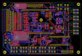
I finalized the PCB (mainly the silkscreen texts for the connectors and some minor modifications here and there):

pcb.png

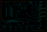
And with only the top silkscreen layer for more clarity:

pcb_slk.png

The 3D views:

3d_pcb_top.png

3d_pcb_btm.png

Hi-res versions :


I also attached the last version of the schematic as it has changed a bit during the PCB routing (mostly some pin and gate swapping).
 

Attachments

  • BO_BMSB_1630.pdf
    282.6 KB · Views: 7
Last edited:
One step closer to manufacturing! Are you planning to just have a pcb or two made then place all components yourself, or have the board manuf. pick n place the and components or?
 
For my 4 BMS I plan to assemble them myself but if there's enough persons interested I can have the board manufactured by a company (just for the SMD stuff as the TH stuff I can do myself pretty easily and quickly so it'll save a lot on the costs of manufacturing and shipping). I don't have pick and place or reflow equipment at home (would like, but the cost...). I've used handsoldering footprints for almost all of the components to ease manual assembly.
 
Last edited:
So today I started the DPB schematic. There's not a lot for now because I imported, modified, created some components and footprints.

@cass3825 I also made a template for the connectors positions, it should be useful for your active balancer board. Of course you can ignore the two 20 pin SIL sockets as they are for the HWP board.

The balancing board goes under the BMS board and is separated from it by 10 mm spacers (maybe a bit more, I need to have the connector in hands to see exactly what is the insertion depth), note there's some components on the bottom side of the BMS board, a rough estimate tells me to keep the components on the balancing board to a height of less than 5 mm to not have problems. The holes are for M3 bolts.

The board to board stackable connector is this one and the other one is this one. Both must be installed on the bottom side (like on the BMS board).

Both +BATT and +5V are fused and protected by TVS diodes. You can use a few hundred mA on +BATT if needed but the power on the +5V is very limited, using no more than 50 mA would be nice and less is always better of course. +BATT can go from 20 V to 64 V (1.25 to 4 V per cell).

SDO must be connected to the output of the second 8 bits shift register of the balancing board as it goes to the HMI board. The 16 bits are shifted cell 0 first and cell 15 last so the first shift register handles cells 8 to 15 and the second one handles cells 0 to 7. Aaaand I just realised something: how do you know which cell gives power and which cell receive power? because I designed this com for the passive balancer where only one cell at a time is balancing. One possible solution: 4 shift registers instead of 2. 2 to select the giving cell and the other 2 to select the receiving cell.
 

Attachments

  • Template.zip
    27.2 KB · Views: 0
  • BO_DPB_1630.pdf
    44.7 KB · Views: 3
So today I started the DPB schematic. There's not a lot for now because I imported, modified, created some components and footprints.

@cass3825 Aaaand I just realised something: how do you know which cell gives power and which cell receive power? because I designed this com for the passive balancer where only one cell at a time is balancing. One possible solution: 4 shift registers instead of 2. 2 to select the giving cell and the other 2 to select the receiving cell.
I’m planning on 4 shift registers, 2 for the high cell and 2 for the low cell. An oscillator will toggle between the pair to allow the high cell to charge the caps, then allow the caps to discharge into the low cell.
 
Ok, we had the same idea apparently :)

So let's agree on the com: first 16 bits to select the giving cell and the last 16 ones to select the receiving cell; is that ok with you?
 
Back
Top