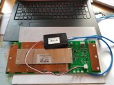
I bought a smart BMS board with Bluetooth advice and UART box with some other parts from AIiexpress, IC GOGOGO Store.
4S 12V Lifepo4 150A Continuous Lithium 3.2V Protection Board Bluetooth APP Computer UART Communication Balance Smart BMS
https://www.aliexpress.com/item/4000249910859.html?spm=a2g0s.9042311.0.0.68d54c4dcQ5S0c
The parts arrived, however, temp. sensors were missing.
Issue resolution, to get adequate response from the shop to close out open issues ihas been somehow difficult due to limited English communication.
After some initial set up problems with SW file re-naming, file unpacking and installation problems I got the
Xiaoxiang APP running and JBD tool software working on my PC.
Many thanks to Hackaday.io, I was able to download the JBD user manual which is a great help.
The BMS board chas been connected to 4x 3,2V in series LiFeP04 CALB cells, the Xiaxiang APP shows me false current reading. The displayed discharge current in APP is about one decimal digit smaller than the true measured current. The Xiaxiang APP doesn’t allow any adjustments for current.
Connecting the UART tool to the board I see the same readings. Current display is about 1/10 smaller than real measurements.
However, the JBD software has a calibration tab which allows calibrating the current flow for idle-, charge-, and discharge current
Any difference to the real current readings should be corrected with this tool.
When the battery draws discharge current the JBD software reads the current as charging current gives an error message not accepting the entry in the discharge box.
Has anybody experienced this kind of an issue on current offset and can guide me how to overcome this issue.
I case th
Thank's,
Waldemar
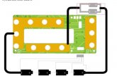
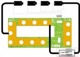
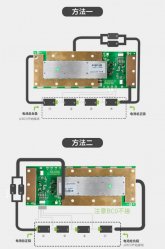
N.B.: With the wiring hook up, I started the balancing cable connection with the black cable to the main negative batt terminal and so on. The B- lead goes to the BMS B- and C- switches the negative to the consumer. Based on the wiring installation everything should be correctly connected.
some pictures see below:
