Had a JK arrive a few days ago, failed to see cells 8 and 9 as soon as it was turned on. Cells were all 3.300V +/- 5mv so below the balancing voltage and within a few milli volts anyway. Replacement is on its way after I gave the supplier pics to confirm the cells and harnesses were good to BMS and no pins on the BMS were bent, so it could only be the BMS.
So out of curiosity I opened up the BMS to take a look.
Found some faults.
On Cell 8 balancer the 0.01R resistor had blown.
On cell 9 there is a large solder bridge between the capacitor and the 8 pin SMD pad, giving a direct route bypassing the cap.
I assume that if I can fix these issues then it may work, there is a spare resistor as there are 2 paths for Cell 8 which I can move to replace the blown one. I have a hot air soldering gun and a soldering microscope so can do that and remove the blob.
However I have found 2 more errors on the board that don't seem related to C8 or C9 but could cause issues.
one is a capacitor where a solder blob links the 2 ends making the capacitor bypassed.
This is fixable by removing the solder or replacing the capacitor.
But for the second one I need confirmation as it looks to me that on the balancer side one chip has the capacitor and resistor positions reversed but that may be by design.
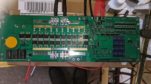
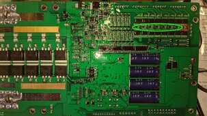
So could someone look at their board and in the red circled area are your caps and resistor orientation matching my pic or the rest of the cell balancers. The first pic is of the full board so you can recognise the board side, second is a close up of the parts that need confirmation, the reversed cap and resistors, resistor top, cap below are in the red oval, in the green oval the rest are all Cap top, Resistor below. If the pics aren't clear I can edit for a close up.


")