


They seem to think it will be much cheaper to produce than current panels, too.
 www.nature.com

 en.shiftdelete.net
High-performance bifacial perovskite solar cells enabled by single-walled carbon nanotubes - Nature Communications
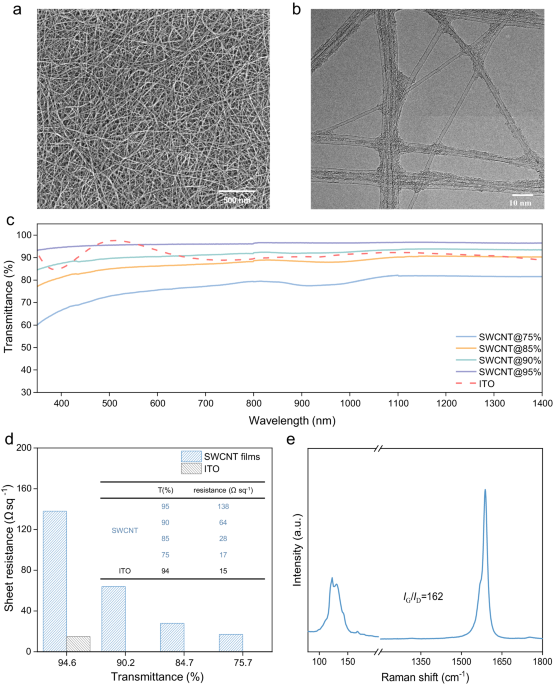
The suboptimal optical transmittance of back electrodes and complex fabrication process hindered development of bifacial perovskite solar cells. Here, authors apply single-walled carbon nanotubes as front and back electrodes, achieving power generation density of 36% and bifaciality factor of 98%.
www.nature.com
Solar panels becoming obsolete! A 70% cheaper alternative is coming
A new type of solar panel alternative with carbon nanotubes and dual-sided features offers 97% efficiency in solar energy technology.
en.shiftdelete.net


")