That should do a good job of sinking heat out of that area.
It's more for shielding and having a low inductance ground than for thermal reasons, but yea, some thermal conductivity is always welcome on that kind of temperature sensitive circuitry
")
Are you still on the Nano?
An ESP8266 with IIC DAC and eventually IIC IO extenders would be much more adapted to do the job.
It provides natively a WiFi connection, so you don't need to retrofit a networking.
It provides much more RAM/ROM speed and power.
It can be programmed with the Arduino IDE and even provides On The Air reprogramming..
I don't want WiFi (or any wireless com actually) because of two main reasons: reliability and security. That's why I chose ethernet (well, that and the nice features of TCP/IP like the advanced adressing and built-in error correction).
WiFi isn't reliable, especially as my house has reinforced concrete floors and hollow bricks for all the walls, and spans two floors + the basement. Plus I plan to have a lot of other things on that network so I highly doubt a WiFi router will be happy with dozens of nodes.
It's also higly unsecure, basically all important stuff in my house will communicate on that network, I don't want anything wireless for that.
RAM/ROM should be enough, that's also why I chose the Every version of the Nano which has additional RAM and FLASH.
I don't use (that piece of crap that is) the arduino IDE, it can't even handle sub-directories properly. Thanks to that and other things we have people putting all the code in one .ino file which is thousands of lines long of unreadable code. So yea, being able to use the arduino IDE isn't a requirement at all for me.
So I'll maybe use something else than the Nano for a 4s version which is more mobile intented and would be 100 % everyone needs oriented (the current version is still a personal project first that I try to open and adapt as much as possible to fill everyone's needs)
You're still free to not use the ethernet module and then you now have a SPI port to do whatever you want to with it (only constraint is that it's shared with the ADC), you can use it as-is, or add a BT or WiFi module, or bit-bang you own protocol (I2C, RS485, CAN, totally custom, ...).
You have got chips like the INA226 that provide an off-rail "current" measurement up to 40V potential difference and an IIC interface with up to 16 addresses. It provides a very precise factory calibrated 14bit DAC.
However, the "current" measurement is -as always- basically a differential 75 millivolts measurement around a shunt.
If you replace the shunt by a simple voltage divider, you can build a measurement ladder for the voltage of every cell up to, say, +24V battery pack,
So you basically have 6 INA226 to measure the voltage of the cells + one to measure the current for each 24V subpart.
You could even built a 2P/6S BMS with 12+2 INA226 on one microprocessor
It is easy to scale: for 48V or more P, you just use two units, and there is no upper limit.
Well at 2.5 USD in 10 quantities that's 40 USD just for the INA and you still need to add all the support components to that. That's far too expensive, and even more so as it would be far less accurate than my solution. It's also in a PITA package and would take a lot of PCB real estate. And it's power hungry and uses the PITA I2C com.
I like the INA226 for things like what it's meant to do as it does it well and is simpler than having a discrete op-amp with a discrete ADC and Vref, but here it's not well suited at all.
If the microprocessors are ESP8266, you will communicate/programm over WiFi and be completely galvanically separated, so you will not get any potential difference problem.
Ethernet is fully galvanically isolated so no problem here.
The presentation of the information could be done in the cloud, so you just need no hardware.
Define "in the cloud" in this context please.
Also if it means internet connected then no, again, security means air-gapped from internet connected networks. When I see industrial plants control panels indexed by google I can tell you it's a (very (super)) bad idea to connect that kind of devices to internet.
The solution with one INA per cell (plus one for the current) is the most accurate and the fastest, but not the only one:
Actually no, the INA is far less accurate (tempco of 10 µV/°C vs 0.3 µV/°C, gain error of 0.1 % vs 0.01 %, ...).
Indeed, we can do it much simpler, cheaper and easier:
We just use the fact that we have a ladder of power cells to wire a comparator between every pair of cells.
We don't need to be fast, if we check the cells at night, with no load or a constant load the voltage wouldn't change that fast.
After the first sweep, we have the approximate voltages, so the next measuring cycles will be just around the the last known cell values.
That could be done much faster.
The bottom high-voltage op-amp will provide a voltage reference from 0v to Vcc depending on the PWM output and the value of R10.
With an ESP8266, you can provide 1024 steps of PWM.
The schematic shows the first 4 cells; you can replicate the top with additional comparators, until you have all the cells you need.
The voltage at A0 will make a clear step each time the comparison voltage will exceed the battery voltage of the next cell, so you can get the voltage of every cell upon one iteration. There is no need to do a multiplex, nor to use a lot of exotics chips...
and you do all the stuff with two I/O pins only...
Well that's one op-amp per cell + a few support op-amps so I don't see how it's simpler, cheaper and easier than having 2 MUX and 3 op-amps for 16 cells.
It also adds a big error term because of the diodes on the output of the op-amps (you basically add a temperature sensor in series with the signal...). And I can't see how it would work as the op-amps are in open loop mode.
Also PWM in a sensitive analog measurement circuitry? that's the last thing I want. And 1024 steps is not good enough so you would need an additional DAC.
But thanks for the ideas, it's always interesting to see other solutions to a problem
Edit: well, you totally changed your last post so I'll answer to it again:
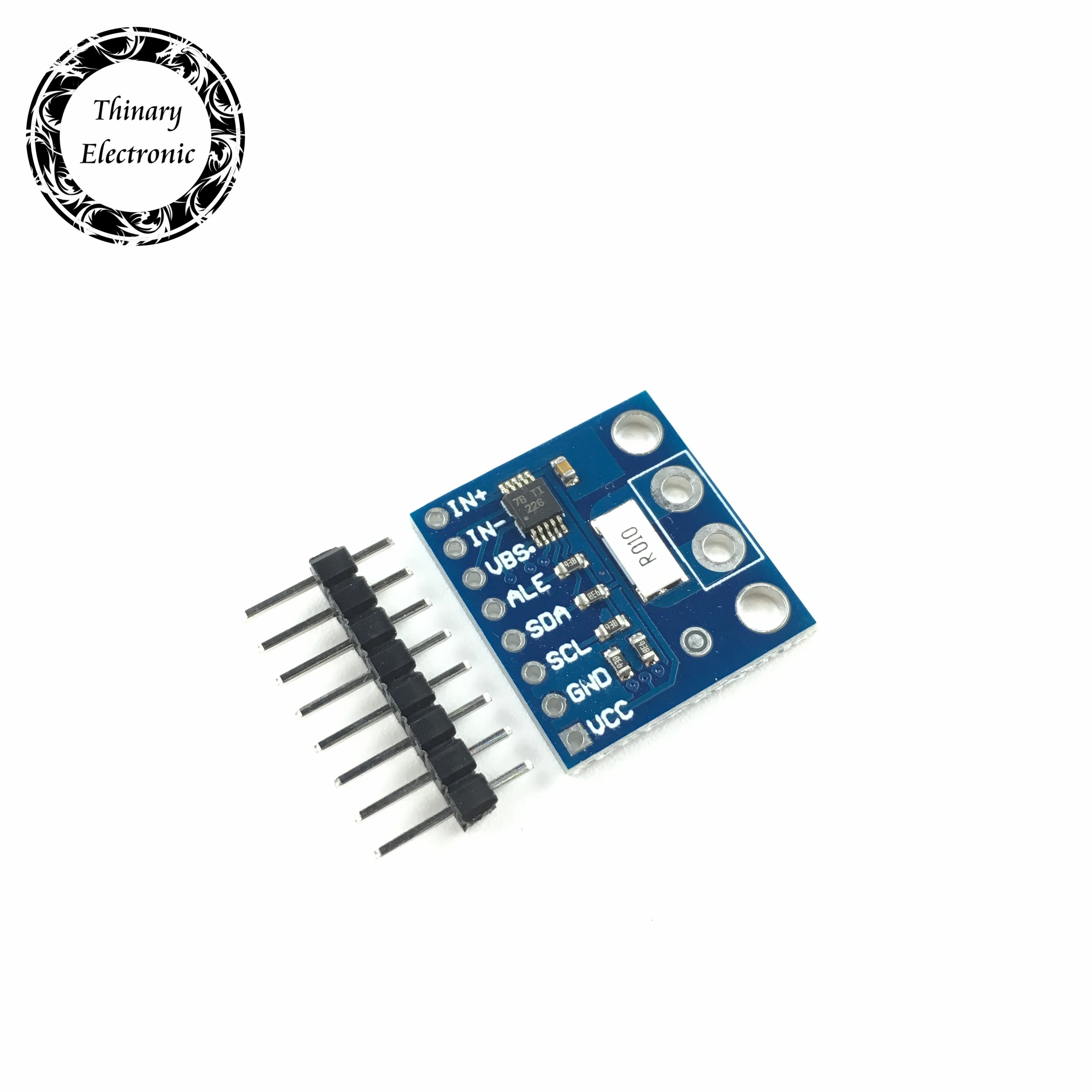
The INA226 can be purchased as finished modules:
Smarter Shopping, Better Living! Aliexpress.com

www.aliexpress.com
I would just modify them, desolder the shunt, solder a voltage divisor instead, solder the address bridges.
Then, all modules can be wired in parallel vertically, bus-wise, you don't even need a PCB.
For a 24V LiFePo with 8 cells, you would need 8 cell INA226 modules, plus one -unmodified, for the current and the total voltage.
Together with an ESP8266, the whole BOM will be under 20€.
x2 if you need 48V...
I'll not buy components from aliexpress for this project. They're almost all factory rejects or fake copies not meeting the original specs in either case.
So that's 40 € for just the cell voltages and current measurement on a 16s pack, with fake components and no scalable manufacturing (desoldering chips isn't realistic beyond a few units). I'm at around 30 € with my current solution, with top tier components and proper manufacturing method, and at least an order of magnitude better accuracy ?
I already spent hundreds (actually I'm pretty sure I'm over a thousand at this point) of hours on the design, component selection, etc... optimizing everything I could, so it'll be hard to do better (I wish a magical better and cheaper solution would exist, but yeah, not gonna happen... ?).