diy solar

diy solar

DIY BMS design and reflection

Well, we can go up to 80 V so that gives 16 V (max is 64 V) which is always better than 10.
yes, it helps a bit but there are always other inductances and drops, it doesn't feel safe to me to have no margin.
I'm not sure about that.
It is. You can imagine when you clamp exactly to battery voltage minus resistive drop. The flow into clamp will not stop and battery is feeding clamp's dissipation. It is very similar compromise you do when designing flyback clamp - you want maximal overvoltage you can afford (limits are secondary diodes) to counteract leakage inductance as fast as possible. And similarly for low clamp voltage you dissipate also voltage reflected from secondary.
That sounds expensive and convoluted.
Yes it is. Nightime cry of despair ;)
I had an idea: we're trying to add a FET to clamp the spike but we already have quite a few FETs that are very capable (each can handle 300 A for seconds if needed, so 3 kA minus some margin to account for uneven load sharing) so why not use those? The only problem is the already in-circuit gate driver but I'm pretty sure it's a solvable problem.
Are you thinking of stop FETs abruptly and when we measure big voltage over them then open them a bit in feedback to clamp it ? Or to join it into single action, rate limit closing of FETs by limiting maximal voltage over them.
It is what I have done now. I used fixed ramp over 1us to minimize overvoltages. But still FETs were blown. It is elegant solution with these drawbacks:
1/ Vth is badly controlled parameter in FETs; once you parallel FETs and use them in active region (as opposed to self-stabilizing saturation region) there will be big differences in current between them, probably leading to cascade failure; solution is either source ballast resistors (not viable here) or feedback driver per FET

2/ I'd like to avoid meddling with main switch FETs in linear mode (I planned to do it for precharge before but now I think more of PWM precharge) because failure of single FET means no protection of battery. And quite likely sequence is: inverter's main resistive divider fails (there is second comparator for big overvoltage) -> it starts to overcharge battery at normal current (no fuse will fail) -> BMS detects and instructs disconnect -> slow switch close and inverter continues to increase output voltage as response (up to 63V safety limit of my one) -> one fet fails -> battery catches fire later; I somehow feel the FETs are quite critical and I should do my best to make sure I prepare them suitable working environment - or maybe I'm just too paranoid :cool:

3/ testing; the clamp I designed above is crude idea. It needs to be verified under various currents, voltages, slew rates, presence of AC on voltage bus, components tolerances; when you combine this with need to cope with 2 anti-series FETs, per FET Vth control, and extra control from MCU then validating it starts to look like man-months projects itself; I'm not afraid of complexity in non-critical areas but this is going to be real time hog
 
It is. You can imagine when you clamp exactly to battery voltage minus resistive drop. The flow into clamp will not stop and battery is feeding clamp's dissipation. It is very similar compromise you do when designing flyback clamp - you want maximal overvoltage you can afford (limits are secondary diodes) to counteract leakage inductance as fast as possible. And similarly for low clamp voltage you dissipate also voltage reflected from secondary.

Ok, I see ;)


Are you thinking of stop FETs abruptly and when we measure big voltage over them then open them a bit in feedback to clamp it ? Or to join it into single action, rate limit closing of FETs by limiting maximal voltage over them.

First option, both because I designed it to open the FET really fast, and because I think it's safer and reduces the energy dissipated in a short for example.


1/ Vth is badly controlled parameter in FETs; once you parallel FETs and use them in active region (as opposed to self-stabilizing saturation region) there will be big differences in current between them, probably leading to cascade failure; solution is either source ballast resistors (not viable here) or feedback driver per FET

Yes but it should work with sufficient margin. And all FETs would be from the same batch which should help.


2/ I'd like to avoid meddling with main switch FETs in linear mode (I planned to do it for precharge before but now I think more of PWM precharge) because failure of single FET means no protection of battery. And quite likely sequence is: inverter's main resistive divider fails (there is second comparator for big overvoltage) -> it starts to overcharge battery at normal current (no fuse will fail) -> BMS detects and instructs disconnect -> slow switch close and inverter continues to increase output voltage as response (up to 63V safety limit of my one) -> one fet fails -> battery catches fire later; I somehow feel the FETs are quite critical and I should do my best to make sure I prepare them suitable working environment - or maybe I'm just too paranoid :cool:

Yea, you should always take some margin on everything. I usually take the worst case (like Tj = 175 °C, etc...) and add some margin on top just to be sure ;)


3/ testing; the clamp I designed above is crude idea. It needs to be verified under various currents, voltages, slew rates, presence of AC on voltage bus, components tolerances; when you combine this with need to cope with 2 anti-series FETs, per FET Vth control, and extra control from MCU then validating it starts to look like man-months projects itself; I'm not afraid of complexity in non-critical areas but this is going to be real time hog

Yep, of course it's not the final design, but it's fine, we're not there yet, no point optimising now something that may not be viable in the end.

Well, with anti-series you can recitify whatever voltage you want to detect and command both FETs at the same time (I assume a local ground for the detection and command circuit that is referenced to the mid-point here) so you only have one detection and control circuit while protecting in both directions.


NB: switch open = no current flow, switch closed = currrent flows. I think you use the terms the other way around so we need to be careful about not misunderstanding what each other says.
 
Yes but it should work with sufficient margin. And all FETs would be from the same batch which should help.
Have you tried it ? I've just taken 2 IPP019N08N from the same lot. One needs 3.7V for 100mA and other 3.4V for 100mA. Because of gfs>110S at 100A difference 0.3V means >33A, actually looking at disgram 6 it is difference 100 vs 180A. And this is for 0.3V diff, DS actually shows range 1.6V for Vth which is 50A vs 400A.
This is problem of nonuniform doping over wafer, mask alignment etc (at least in ASIC but I guess it is similar in power mosfet technology). When I needed same Vth in ASIC design I had to use interdigitized structure of fets.
Yea, you should always take some margin on everything. I usually take the worst case (like Tj = 175 °C, etc...) and add some margin on top just to be sure ;)
after I lost a few expensive FETs on my latest 7kW BLDC driver for CNC I found it is not overkill to oversize FETs by 50%-100% :) Top DS parameters are measured at clean setup by manufacturer - exceptionally good cooling, no overshots..
NB: switch open = no current flow, switch closed = currrent flows. I think you use the terms the other way around so we need to be careful about not misunderstanding what each other says.
I think I use the same logic, where did I messed it ?
 
Have you tried it ? I've just taken 2 IPP019N08N from the same lot. One needs 3.7V for 100mA and other 3.4V for 100mA. Because of gfs>110S at 100A difference 0.3V means >33A, actually looking at disgram 6 it is difference 100 vs 180A. And this is for 0.3V diff, DS actually shows range 1.6V for Vth which is 50A vs 400A.

Nope, not yet, hence the "should". In theory I could test and match FETs for Vgsth, it's not like I'll make millions of BMS. Of course it would be easier not to, but if it's the only PITA thing to do to solve that damn inductive spike problem then it's worth it (it's the only problem in the whole thing I couldn't solve to my liking so far).


I think I use the same logic, where did I messed it ?
Here I think:
Are you thinking of stop FETs abruptly and when we measure big voltage over them then open them a bit in feedback to clamp it ? Or to join it into single action, rate limit closing of FETs by limiting maximal voltage over them.
 
Nope, not yet, hence the "should". In theory I could test and match FETs for Vgsth, it's not like I'll make millions of BMS. Of course it would be easier not to, but if it's the only PITA thing to do to solve that damn inductive spike problem then it's worth it (it's the only problem in the whole thing I couldn't solve to my liking so far).


Here I think:
Yes you are right :rolleyes: I was somehow visualizing it as "flow" and thinking of valves. Thanks for catching this.

Regarding clamping, somehow I'm close to use bunch of TVS. I'll probably modularize my 8-channel switch to have one "strip PCB" per channel with 3x 5kW 51V TVS on both FET sides, 1mR+INA181 measuring, MIC4128 gate drivers and local STM32G051G per strip. Strips can be screwed to common busbars (GND and C+) and powered from central DC-DC with cheap (750313723) xformers. Comm using optocoupled shared UART. Each strip locally grounded to connected FET sources.
It allows me 1us reaction from sense resistor to gate drivers using internal failsafe MCU comparators and timer. Each channel has 40A 2520 SMD fuse so that I set limit 100A/chan and expect up to 150A at time of off event. 3x TVS is good for 180A for 1ms with 80V limit.
I would use 100V (and probably will in later variations) but I already bought 100pcs SIR582..
 
Just FYI I designed another way to keep FETs off before drivers take over - BSS139 (depletion fet) from gate to GND and BSS gate connected to dual BAV99+2x10nF negative voltage generator from MCU timer pin...
BSS139 is on without power.
 
In theory I could test and match FETs for Vgsth, it's not like I'll make millions of BMS.

Unless it needs to operate in a "strategic" environment, where neutron flux will alter doping and cause serious divergence in your carefully matched threshold voltages. ;)

But then you'd also have problems like shoot through when everything turns on for a while. RTL, Resistor-transistor logic, KISS.

The mismatch of FETs was one reason I went with BJT for an RF amp in an instrument, when trying to make a class-A output stage. Not at all applicable to your inverter/BMS power levels.

Are you trying to balance current for an impulse, like surge or inductive kick? Or for steady-state operation?
How about something like thermistor responding to FET temperature and altering gate bias? Instead of a current sensor, it is a power/temperature sensor.
 
Regarding clamping, somehow I'm close to use bunch of TVS. I'll probably modularize my 8-channel switch to have one "strip PCB" per channel with 3x 5kW 51V TVS on both FET sides, 1mR+INA181 measuring, MIC4128 gate drivers and local STM32G051G per strip. Strips can be screwed to common busbars (GND and C+) and powered from central DC-DC with cheap (750313723) xformers. Comm using optocoupled shared UART. Each strip locally grounded to connected FET sources.
It allows me 1us reaction from sense resistor to gate drivers using internal failsafe MCU comparators and timer. Each channel has 40A 2520 SMD fuse so that I set limit 100A/chan and expect up to 150A at time of off event. 3x TVS is good for 180A for 1ms with 80V limit.
I would use 100V (and probably will in later variations) but I already bought 100pcs SIR582..

It's becoming hard to follow text only infos given the number of components and connections but I see the general idea.


Just FYI I designed another way to keep FETs off before drivers take over - BSS139 (depletion fet) from gate to GND and BSS gate connected to dual BAV99+2x10nF negative voltage generator from MCU timer pin...
BSS139 is on without power.

Oh yep, I also saw BJT based schematics but I wanted a passive solution as much as possible.


Unless it needs to operate in a "strategic" environment, where neutron flux will alter doping and cause serious divergence in your carefully matched threshold voltages. ;)

? I should be fine in that department ^^


Are you trying to balance current for an impulse, like surge or inductive kick? Or for steady-state operation?
How about something like thermistor responding to FET temperature and altering gate bias? Instead of a current sensor, it is a power/temperature sensor.

Yes, inductive spike due to wire inductance when opening the FETs for the e-fuse feature. Thermistor would be far too slow here.

If you have a good idea on how to clamp the peak to less than 80 V (with a normal working voltage of 64 V) when interrupting 1 to 1.5 kA passing through a 0.1 to 10 µH inductance I'm all ears ;)
 
Clamp wire on which side of FET? Is this a wire from BMS positive terminal, driving load?
In that case, when FET opens I think inductance of wire causes voltage to fly negative. In that case, just use a (fast) diode to clamp it to battery negative.
Same circuit as a buck converter.

i.e. take a look at the polarity of the spike you're trying to clamp.
You need to clamp both polarities on both switch sides ;)
 
Or is that one polarity on one switch side, one polarity on the other? I would think inductance and stored energy in cable coming from cells is under your control and more limited. Routing of negative cable could reduce loop area (even trace back along busbars to positive terminal. Depending on cell orientation and arrangement, busbar inductance could be minimized. Jelly roll length is outside your control but

I guess if you disconnect when outside is charging, then the voltage flies positive. But that won't be massive fault current. Typical snubber for spike. If it goes 10V higher than battery (e.g. SCC failed shorted), could clamp to ground (short it), but turn off both directions of BMS MOSFET first, not just charging path.

But I think most severe spike you have to deal with is opening from a short, possibly 10kA or more, with most kick being on load side and going negative.
 
Clamp wire on which side of FET? Is this a wire from BMS positive terminal, driving load?
In that case, when FET opens I think inductance of wire causes voltage to fly negative. In that case, just use a (fast) diode to clamp it to battery negative

Wire on the load side, BMS is on the battery negative. The BMS switch is bidirectional, you can't assume a polarity.

All the parameters are at the end of my previous post: https://diysolarforum.com/threads/diy-bms-design-and-reflection.4065/page-35#post-887063 You can't by-pass those and you can assume just a simple inductor powered by a constant voltage source set to 64 V, you don't need to bother about if it's powered by a SCC, battery or whatever. The solution must be practical (especially size-wise) and as low cost as possible.

See why it's a very hard problem solve?
 
Wire on the load side, BMS is on the battery negative. The BMS switch is bidirectional, you can't assume a polarity.

But I think in one direction, current is much lower. Whatever charger can deliver. 100A per 5kW.

Only in the discharge direction will it be 1kA or 10kA, so only one polarity of voltage spike is so massive. I think that polarity can be clamped with diode to opposite rail.

The smaller kick when current comes from charging source - if it kicks 10V beyond battery voltage (because BMS is now open), how about crowbarring it to opposite rail with a FET?
 
But I think in one direction, current is much lower. Whatever charger can deliver. 100A per 5kW.

Only in the discharge direction will it be 1kA or 10kA, so only one polarity of voltage spike is so massive. I think that polarity can be clamped with diode to opposite rail.
You can (should) assume symmetric source/load on both sides. Because you can e.g. connect more BMS to common inverter, you can need longer battery cables and you can have short at battery side. And you also want to keep max rating docs simple for user.
Also inverter have something like 10-100mF caps, this can cause massive positive overcurrent too.
So that both sides need freewheeling diodes from negative to positive (handles one direction of kick) and both sides needs some path to conduct other polarity of kick.
The smaller kick when current comes from charging source - if it kicks 10V beyond battery voltage (because BMS is now open), how about crowbarring it to opposite rail with a FET?
Crowbarring cable inductance causes even more current (albeit on lower voltage over BMS) from massive inverter caps and hopefully opens some fuse soon. My experience of such short is permanent offset of inverter battery path current probe (probably partial permanent magnetization of permaloy core in Lemo sensor?).
Also I would utter some not so nice words about BMS which blows fuse every time I turn battery off under (even partial) load.
 
As I previously suggested (CAP+FET switched resistor), I just found it is reportedly used in automotive to control inductive load dumps. See
this link for example.
Probably this is most joule-capable way we can devise and also is quite small area comparing to TVS or FET arrays.
 
But I think in one direction, current is much lower. Whatever charger can deliver. 100A per 5kW.

Only in the discharge direction will it be 1kA or 10kA, so only one polarity of voltage spike is so massive. I think that polarity can be clamped with diode to opposite rail.

The smaller kick when current comes from charging source - if it kicks 10V beyond battery voltage (because BMS is now open), how about crowbarring it to opposite rail with a FET?

Again, you can't by-pass the parameters I gave; trust me, I tried...


You can (should) assume symmetric source/load on both sides

Yes, exactly.


Also I would utter some not so nice words about BMS which blows fuse every time I turn battery off under (even partial) load.

While one of the main point of having a e-fuse is to not blow the expensive class T or similar fuse ?


As I previously suggested (CAP+FET switched resistor), I just found it is reportedly used in automotive to control inductive load dumps. See
this link for example.
Probably this is most joule-capable way we can devise and also is quite small area comparing to TVS or FET arrays.

Yep, that or 100 V FETs + TVS if that's cheaper. Thanks for the pdf, I'll read it when my brain is less mushy than currently ;)
 
Yep, that or 100 V FETs + TVS if that's cheaper. Thanks for the pdf, I'll read it when my brain is less mushy than currently ;)
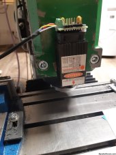
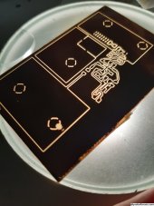
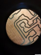
I finished CAN controlled UV laser for my CNC so that as test I created PCB for that cap+FET, we will see :)
20231005_005856.jpg 20231005_005845.jpg 20231005_005819.jpg
 
Any hazards from specular reflection? Safety provisions?
 
I'd drop a cover over it. Interlocked.
Invisible beam.
Add a camera for monitoring, or a viewport with suitable filters.
Refer to the safety triangle, you're at the point, "PPE".
 
Back
Top