diy solar

diy solar

DIY BMS design and reflection

It was meant as cost optimization (but as software guys would say - maybe it is premature optimization). It seems you want to stay with 80V fets so I got you want best Rds for given price and not pay extra for 100V.

Both the models you've quoted are 100 V, so I'm a bit lost. I don't really want to stay at 80 V, it's just that cost (or losses) increase a lot if I go for 100 V.


If you forget about efficiency you can get away with two pairs of 3mR fets with wide SOA - enough for on/off event. But as downside you have 270W loss at 300A.
So that solve this second problem with bunch of cheap FETs with decent Rds but with inferior SOA - these are much cheaper.

They are much cheaper because they are 3.3 mOhm Rdson, mine are 1.1, so you would have 3 times the losses.


Given you already have MCU, it cost only one extra driver. But probably I see it in different light as I already have 16 drivers on my PCB.

I ran out of I/O on the MCU ^^ A next version will definitely have one more mux to solve the I/O limitation.
 
Both the models you've quoted are 100 V, so I'm a bit lost. I don't really want to stay at 80 V, it's just that cost (or losses) increase a lot if I go for 100 V.
Ehh sorry, I was looking for new 100V fets for my use and used them as example. When looking at 80V interestingly there is no one which is cheaper just because of smaller SOA with reasonable Rds. My fault.
But SQJQ184E might interest you. 1.1mR, wide SOA and half price...

For me, I just ordered NVBGS4D1N15MC, 150V, 3.3mR typ, 2500A/100V/1us peak or 1000A/50V/10us. And for EUR 4 at Farnell. I don't know what to do with them but they seems too good to not have them here :cool:

Also have a look at Vishay TVS. They quote both 1ms and 20us transient in DS. 60V one clamps to 96V at 51A and 125V at 320A. Costs about EUR 0.3. With 20 pieces in parallel you could guarantee to be under 100V at 1kA pulse but 80V seems impossible.
I plan to use 51V one - 4pcs in parallel keeps me under 100V @ 1kA and will change from 80V to 100V fets. With 20pcs of 51V you should be safely under 80V up to 1.2kA...
 
Last edited:
Ehh sorry, I was looking for new 100V fets for my use and used them as example. When looking at 80V interestingly there is no one which is cheaper just because of smaller SOA with reasonable Rds. My fault.

Ok, no worries ;)


But SQJQ184E might interest you. 1.1mR, wide SOA and half price...

Thanks.


Also have a look at Vishay TVS. They quote both 1ms and 20us transient in DS. 60V one clamps to 96V at 51A and 125V at 320A. Costs about EUR 0.3. With 20 pieces in parallel you could guarantee to be under 100V at 1kA pulse but 80V seems impossible.
I plan to use 51V one - 4pcs in parallel keeps me under 100V @ 1kA and will change from 80V to 100V fets. With 20pcs of 51V you should be safely under 80V up to 1.2kA...

I'll look into the power zener solution because that seems the most promising path so far. Getting pulse data on BJTs will be the biggest PITA here I think.
 
I'll look into the power zener solution because that seems the most promising path so far. Getting pulse data on BJTs will be the biggest PITA here I think.
Can you elaborate ? You mean something like nte5240a or zener with BJT as amplifier ?
 
I've suggested exactly that to a colleague making a test board (collector or drain to supply, emitter or source to load). Powered from bench supply, reverse polarity or up to 32V might accidentally be applied. Preferable to withstand without damage. In this case, zener and transistor as regulator can drop the additional voltage, doesn't need to clamp. The zener might have tried to dissipate 25V x 1A or 3A if used by itself.

Your application maybe does need to clamp, so emitter or source to ground. I've used that as shunt regulator for old motorcycle, which had been designed to have FLA battery do the clamping. I used zener and darlington.
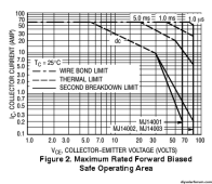
But here you can't use series BJT regulator because of Vsat (whole point of FET use) and using it to clamp will be also problem. That is because if you bias PNP base to say 55V, collector to GND and emitter to clamped line then you get whole current (1000A pk) redirected to emitter. I have yet to find BJT so big. I used MJ14001 for this, here is the SOA:
screendump.29.png
As you see you don't get larger current for short pulses because of secondary breakdown. This breakdown is not present in FETs - at least older ones, when you have FET with high transconductance then it is there too.
IGBTs can be used for 1kA but not in linear region (needed for the clamp).
I don't see other ways except:
- use FET's avalanche - I don't like it, energy in 10m cable is larger than typical avalanche rating
- use RCD snubber - actually used in some automotive BDUs to slow dV/dt
- use MOSFET/IGBT connected ballast pulse resistor - but how big ? R-2R network of 3 of them ?
- zener/TVS/MOV etc to clamp
- active linear FET clamp (I used IXTK200N10L2 for this, it can clamp 500A to 60V for 25us but is a bit expensive)

In any case don't forget you need freewheeling diodes on both sides of switch. With TVS or FET-clamp you have them for free.
 
Can you elaborate ? You mean something like nte5240a or zener with BJT as amplifier ?

Zener + BJT ;)


As you see you don't get larger current for short pulses because of secondary breakdown.

Here the limitation would be the bond wires, not the secondary break down. If we can find FETs that are kA pulse capable I'm pretty sure we can find BJTs too.
 
Zener + BJT ;)


Here the limitation would be the bond wires, not the secondary break down. If we can find FETs that are kA pulse capable I'm pretty sure we can find BJTs too.
You are right with bond wire limit. I asked my IGBT friend for big BJTs. He has some, but we concluded it is no way to use them in linear mode. Biggest one - QM1000HA-2HB darlington (hard to get it these days and cost over EUR500) can do up to 2kA if you maintain base current 50A. But is specified only for pulse mode (and 2.5us rise time).
ST used to make rather fast ESM2012DV (180Apk) but it is obsolete now.
Or parallel 20xMJ14001 with 10mR emitter ballast. Base current (100A pulse) can be handled by zener+capacitor. But it is EUR200 total..

IMHO the benefit of FET is positive tempco of channel. It tends to make current homogenous. On other side in BJT once you go over some current density there is forming of current "filaments" (dont remember physic behind it) which leads to hotspots. Almost all FETs have high pulse/steady ratio (typ. 10), but all BJTs I've seen have max 2 (more typically 1).
 
Last edited:
Bond wires have a continuous current limit, heating and thermal dissipation (familiar ampacity) and in the case of aluminum metal migration. A 1 mil wire typically is pushed to the limit around 1 amp. Sometimes you see that mentioned in reports on test setups for substrates and devices. How well it works depends on wire length (conducted thermal path). Power devices may have many wirebonds in parallel, or ribbon bonds.

For pulses, current could go higher but there is a Joule limit given that heat doesn't have time to flow anywhere. Very excessive current and you get arc blast; for a wire bond about 1000V at 1000A or 1 microsecond (1 Joule) and you have a nice little detonator, able to create a shock wave and set off ordnance.

These limits and effects could come in to play for fault currents and surge events. Hopefully not repetitive.

Flip chip power devices would eliminate the wirebond, but I'd think it makes thermal path to PCB worse. Maybe some have backside bond for heatsink as well.

 
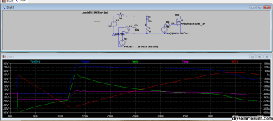
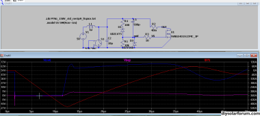
If you want to create active clamp, the NVBGS4D1N15MC mentioned above with zener and some phase compensation might do it. Probably 2 in parallel because with low overvoltage it takes longer to push inductive current down. ON has nice models, I did quick and dirty test. The compensation is more complex than for BJT but all other measures are superior IMHO.
screendump.30.png
 
Bond wires have a continuous current limit, heating and thermal dissipation (familiar ampacity) and in the case of aluminum metal migration. A 1 mil wire typically is pushed to the limit around 1 amp. Sometimes you see that mentioned in reports on test setups for substrates and devices. How well it works depends on wire length (conducted thermal path). Power devices may have many wirebonds in parallel, or ribbon bonds.

For pulses, current could go higher but there is a Joule limit given that heat doesn't have time to flow anywhere. Very excessive current and you get arc blast; for a wire bond about 1000V at 1000A or 1 microsecond (1 Joule) and you have a nice little detonator, able to create a shock wave and set off ordnance.

These limits and effects could come in to play for fault currents and surge events. Hopefully not repetitive.

Flip chip power devices would eliminate the wirebond, but I'd think it makes thermal path to PCB worse. Maybe some have backside bond for heatsink as well.
It is interesting. I wonder why in big BJTs for small voltages they say bondwire is the limit while MOS is able to provide 10x higher current in the same package. Are the bonds so different between BJT and MOS ?
 
You are right with bond wire limit. I asked my IGBT friend for big BJTs. He has some, but we concluded it is no way to use them in linear mode. Biggest one - QM1000HA-2HB darlington (hard to get it these days and cost over EUR500) can do up to 2kA if you maintain base current 50A. But is specified only for pulse mode (and 2.5us rise time).
ST used to make rather fast ESM2012DV (180Apk) but it is obsolete now.
Or parallel 20xMJ14001 with 10mR emitter ballast. Base current (100A pulse) can be handled by zener+capacitor. But it is EUR200 total..

IMHO the benefit of FET is positive tempco of channel. It tends to make current homogenous. On other side in BJT once you go over some current density there is forming of current "filaments" (dont remember physic behind it) which leads to hotspots. Almost all FETs have high pulse/steady ratio (typ. 10), but all BJTs I've seen have max 2 (more typically 1).

Yea, might be a good idea to replace the BJT by a FET.


If you want to create active clamp, the NVBGS4D1N15MC mentioned above with zener and some phase compensation might do it. Probably 2 in parallel because with low overvoltage it takes longer to push inductive current down. ON has nice models, I did quick and dirty test. The compensation is more complex than for BJT but all other measures are superior IMHO.
View attachment 170109

Where is V(d) measured? Why not put a zener instead of Vout * 0.3?
 
Yea, might be a good idea to replace the BJT by a FET.

Where is V(d) measured? Why not put a zener instead of Vout * 0.3?
Ignore Vd - it is derivative of Vout (by RC), I prepared it because I expected need to add it to control equation to stabilize it. Somehow it was enough to make P term 0.3 (from 1).
I started with zener and PNP-NPN followers but it oscillated. I already did similar circuits and I always needed some lead-lag compensations to keep them both fast and stable. It is faster to make loop stable by spice B device and develop detailed schematic later.
Probably we could try source follower (lower gain, first order system) - I had no more time to test it. Also add 20mR to D or S would be wise to overtake half of power from FET
Edit: I tried to make discrete compensation. Not final solution but working concept:
screendump.31.png
 
Last edited:
Ok, I see.

The FET solution looks very promising. I think it would be better if D3 would be on the other side of R3, directly on the gate.

Good idea on the resistor on the drain, it could even be a trace on the PCB given it's very low.
 
Last edited:
Ok, I see.

The FET solution looks very promising. I think it would be better if D3 would be on the other side of R3, directly on the gate.

Good idea on the resistor on the drain, it could even be a trace on the PCB given it's very low.
Yes, probably R3 is not necessary, it is mainly to help spice solver. The FET model is encrypted and probably models many parasitics because it tends to oscillate wildly without a bit of damping. I'll try to breadboard it later.
The collector resistor would be best low inductance wire type, I'd use OARS1R040JLF which is actually pulse rated.
 
I didn't knew that was a thing, a bit ridiculous from them to do that if you ask me...
Yes, it prevents me to simplify it and/or run it via opensource ng-spice..
Ah yep, quite a high energy rating too, that's nice.
I like to use them for current sense in big motor controllers :)

But .. and please prove me wrong .. The problem seems worse than I thought. Assume you have longest cable with 10uH, 62V bat and start acting on 1300A overcurrent. You close FETs and clamp voltage to say 72V. So that you impose 10V to the cable and it will take 1.3ms to go from 1300A to zero. Note that part of energy to dissipate is from cable but part is still fetched from battery. So that the clamp must support 650A * 1.3ms for average. That is out of SOA of FETs and TVSes.
Duh. I'll think more about it.
What about simple diode from input and output to 50uF WIMA cap (MKS4C054706G00KSSD), and 2kA peak 80V FET with 30mR resistor which would connect the resistor once voltage >75V and disconnect when <70V - hysteretic regulation. There should be quite low dissipation in the FET, cap is rated 2.5V/us but tested at 25V/us (1250A). It might be quite scalable solution
 
But .. and please prove me wrong .. The problem seems worse than I thought. Assume you have longest cable with 10uH, 62V bat and start acting on 1300A overcurrent. You close FETs and clamp voltage to say 72V. So that you impose 10V to the cable and it will take 1.3ms to go from 1300A to zero.

Well, we can go up to 80 V so that gives 16 V (max is 64 V) which is always better than 10.


Note that part of energy to dissipate is from cable but part is still fetched from battery.

I'm not sure about that.


What about simple diode from input and output to 50uF WIMA cap (MKS4C054706G00KSSD), and 2kA peak 80V FET with 30mR resistor which would connect the resistor once voltage >75V and disconnect when <70V - hysteretic regulation. There should be quite low dissipation in the FET, cap is rated 2.5V/us but tested at 25V/us (1250A). It might be quite scalable solution

That sounds expensive and convoluted.


I had an idea: we're trying to add a FET to clamp the spike but we already have quite a few FETs that are very capable (each can handle 300 A for seconds if needed, so 3 kA minus some margin to account for uneven load sharing) so why not use those? The only problem is the already in-circuit gate driver but I'm pretty sure it's a solvable problem.
 
Last edited:
Back
Top