diy solar

diy solar

DIY BMS design and reflection

Introduction

Hello. I've come over this thread recently and I'd like to join the conversation. I started with my BMS about year ago, with different design and probably a different goal but I hope we can share some experiences. I'll try to respond to several interesting points in this thread below.
20230917_121023.jpg
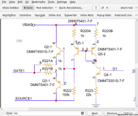
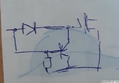
MOSFET opening by high dV/dt has already bitten me. Most new drivers use "miller clamp" so that you don't need to worry but in my BMS I drive 32 mosfets on different voltage levels so that I needed simple/cheap solution:
screendump.27.png
But for existing clamp-less driver it is simple to add one PNP to do it. See e.g. ROHM-clamp-AN.

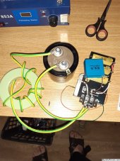
For TVS clamping of wires. Twin cabling has approx 1uH/1m, I have 8m of 2x25mm2 wires and I measured 12uH. I crafted simple tester (see pic below) where I use 15uH/200Asat inductor and big (10mohm ESR) cap plus big 500A (IIRC) mosfet.
20230917_121405.jpg 20230813_022000.jpg
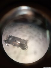
You can see 56V 1.5kW SMB transil - it blowed up at 80A pulse. Then I used THT 5KP51A and it survives 140A and the voltage over it was clamped to 72V. The 1.5K SMB transil was able to clamp only to 110V when still alive. Thus I use 80V MOSFETs too (SiR582).

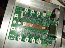
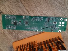
It is possible to buy used or almost new (after minor crash) batteries from EV. It can be expected these will be more available in coming years. I have some 12S 25Ah prismatic ones where I replaced balancer and measurement by own one:
20230917_123158.jpg
It uses ISL94216+STM32L011 and implements isolated Modbus communication.
Because of battery topology (it already has nice big terminals) it is not viable to have disconnector in each battery. Thus my BMS is designed as "multi-connector" for many batteries where each input is capable of 20A (30A peak) and has main FET switch with isolated current measurement (ACS711KE) and extra precharging branch with smaller/cheaper FETs. This branch is connected to external 2R2/20W resistor and is used to precharge invertor caps on first connect and to balance newly connected battery if it is more than 0.4V from others. More such boards can be connected side by side and communicate via RS485.
It has 2xRS485 (one co connect to battery balancers, other for inverter or other master device), ethernet and LCD display.
Controlled by STM32F407 with FreeRTOS/lwip/LFS and scriptable by embedded Lua.
If someone is interested I have also done control plugin boards into Infini inverters, fast custom 3phase meter with eth, 60A bidir voltage booster for batteries and now working on 3phase inverter.
M.
 
Last edited:
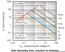
In the last comment I've wanted to introduce myself. I'd like to ask for opinions about mosfet SOA and speed of turn-on/off. There was very nice overview by (IIRC) BiduleOhm. For SiR582 we have SOA:
screendump.28.png
I'm interested if one can extrapolate for shorter pulses than 100us. Basicaly I strive for e-fuse like in BiduleOhm design, just now I use 1k gate resistor fo have about 1us on/off time. I slowed it down from original 100ns because there was too much ringing on the verge of avalanche.
It seems to me that battery turn-on time is dictated by smallest possible wiring inductance on ONE side of switch (I assume single point of failure design so that I expect one side of switch can be shorted but not both).
For 1uH (1m) minimum we have for 60V rise 60A/us. If you can switch under 1us you are in the SOA (at 100us power limit line). But if I could extrapolate extra 10us line then I can switch-on over time of 10us which would help ringing...
Regarding turn-off event. ACS711 has 1.3us FAULT delay to overcurrent 31A, it goes to MCU interrupt line, MCU latency is 400ns. So that
over these 2us the current already rise to 150A. Hence I guess turn-off should be as fast as possible. And we need to solve ringing/inductive kick by other means (snubbers, TVS).
Am I correct ?
 
Last edited:
NB: Currently I put this project on pause, it's definitely not abandonned but I'm very busy on other projects, mainly working on my house (it was pretty much only walls and a roof when I bought it so there's lots of work). Once I have those done I'll continue on the BMS, design is almost done and then comes prototyping and testing which will be a big part of the project.


Hello. I've come over this thread recently and I'd like to join the conversation. I started with my BMS about year ago, with different design and probably a different goal but I hope we can share some experiences. I'll try to respond to several interesting points in this thread below.

Different but also similar with the added busbar on the PCB for example :)


MOSFET opening by high dV/dt has already bitten me. Most new drivers use "miller clamp" so that you don't need to worry but in my BMS I drive 32 mosfets on different voltage levels so that I needed simple/cheap solution:
screendump.27.png

But for existing clamp-less driver it is simple to add one PNP to do it. See e.g. ROHM-clamp-AN.

Very interesting to know it is a problem IRL because so far everyone told me it's likely not a problem and that the engineers who wrote the 2 or 3 papers I based my calculations on were splitting hairs.

As you probably saw I solved the problem (at least in theory) by adding a capacitor between the gate and source and a diode (so I can still turn off the FETs as quickly as possible) which I think is the most compact and cost effective way of doing it, especially since a BJT based miller clamp also needs a cap. It's also a design confirmed to work IRL in half and H bridges for the top FET who see the source voltage change quickly when the bottom FET switches, altho they typically use far smaller caps, in the nF range for a few reasons. It's basically rising the Cgs artificially so the Cgd/Cgs capacitive divider has a higher ratio so Vgs can't go above the Vgsth with whatever Vds your design is using.

IIRC the gate driver I used have a clamp but I'm not sure it works when the driver is unpowered. I prefer to have an additional way to solve the problem right at the FET pins (just the track inductance from the driver to the gate can be a problem here given the PCB is quite big) and I planned to run tests anyway to see what happens IRL.

32 FETs? that's a lot, is it for current capability or for advanced features?


For TVS clamping of wires. Twin cabling has approx 1uH/1m, I have 8m of 2x25mm2 wires and I measured 12uH. I crafted simple tester (see pic below) where I use 15uH/200Asat inductor and big (10mohm ESR) cap plus big 500A (IIRC) mosfet.
20230917_121405.jpg
20230813_022000.jpg

You can see 56V 1.5kW SMB transil - it blowed up at 80A pulse. Then I used THT 5KP51A and it survives 140A and the voltage over it was clamped to 72V. The 1.5K SMB transil was able to clamp only to 110V when still alive. Thus I use 80V MOSFETs too (SiR582).

Yep, I added a few big TVS to help the FETs but I still think they will go into avalanche on very inductive loads. Even if I don't like it a lot it should be fine as they are avalanche rated and I don't have another practical solution beside going with higher Vds FETs so only the TVS are conducting on a spike (but it means they would be more expensive and I would need more of them because of the higher Rdson...).


This branch is connected to external 2R2/20W resistor and is used to precharge invertor caps on first connect and to balance newly connected battery if it is more than 0.4V from others.

Interesting. I have a very similar design and I wonder how you determined the 0.4 V threshold? I didn't settled on the threshold I will use yet but was thinking to use the minimal realistic resistance between two packs wired together and the maximum current I want flowing between them to calculate it.


In the last comment I've wanted to introduce myself. I'd like to ask for opinions about mosfet SOA and speed of turn-on/off. There was very nice overview by (IIRC) BiduleOhm. For SiR582 we have SOA:
screendump.28.png

I'm interested if one can extrapolate for shorter pulses than 100us. Basicaly I strive for e-fuse like in BiduleOhm design, just now I use 1k gate resistor fo have about 1us on/off time. I slowed it down from original 100ns because there was too much ringing on the verge of avalanche.

As you can see it's exponential from 10 s to 1 ms but then it doesn't follow the same trend anymore for the 100 µs curve so it'll be very hard to extrapolate. You best bet is asking the manufacturer. But at the 1 µs time scale you probably can assume the Idm will be your limit anyways and that's a hard limit mainly depending on the bond wires, silicon, etc. and not the thermal limit.

1 k sounds very high for a gate resistor (for example I have 20 Ohm for turn-on and 15 for turn-off), those FETs must have a very low gate charge I guess.


It seems to me that battery turn-on time is dictated by smallest possible wiring inductance on ONE side of switch (I assume single point of failure design so that I expect one side of switch can be shorted but not both).
For 1uH (1m) minimum we have for 60V rise 60A/us. If you can switch under 1us you are in the SOA (at 100us power limit line). But if I could extrapolate extra 10us line then I can switch-on over time of 10us which would help ringing...

Yes, exactly. If you can't switch super slowly (like 1 ms) then you're probably running a bit too close to the limit of the FET and I would advise to see if it's ok to get a beefier one. It should make your life a lot easier, for other things too like your SOA problem (but it would cost a bit more of course) ;)


Regarding turn-off event. ACS711 has 1.3us FAULT delay to overcurrent 31A, it goes to MCU interrupt line, MCU latency is 400ns. So that
over these 2us the current already rise to 150A. Hence I guess turn-off should be as fast as possible. And we need to solve ringing/inductive kick by other means (snubbers, TVS).
Am I correct ?

Yes, you're 100 % correct. I basically arrived at the conclusion you can't do e-fuse with the MCU, it's too slow (well in theory you can if you use a crazy fast MCU which would be more a SoC than a MCU at that point...). Doing it in HW is also quite simple (basically just a comparator), you just need to keep the speed in mind for everything in the chain (fast comparator, no low-pass filter, low capacitive loading, good decoupling, ...) but that's pretty much it. I also hate having a something as critical as a e-fuse run in SW (and I'm a SW architect and developper ?).

NB: you can forget the snubber solution (I explored that path too) as it would need LOTs of capacitance (think mF to F, not nF or µF...), it's not practical. Maybe a small-ish one just to help another type of clamp is possible tho.
 
Last edited:
NB: Currently I put this project on pause, it's definitely not abandonned but I'm very busy on other projects, mainly working on my house (it was pretty much only walls and a roof when I bought it so there's lots of work). Once I have those done I'll continue on the BMS, design is almost done and then comes prototyping and testing which will be a big part of the project.
Well I fortunately have the house done (I was reconstructing it 5yrs ago) as I'm starting to be old for this kind of work. But you know, there is always more to do :)
Very interesting to know it is a problem IRL because so far everyone told me it's likely not a problem and that the engineers who wrote the 2 or 3 papers I based my calculations on were splitting hairs.

As you probably saw I solved the problem (at least in theory) by adding a capacitor between the gate and source and a diode (so I can still turn off the FETs as quickly as possible) which I think is the most compact and cost effective way of doing it, especially since a BJT based miller clamp also needs a cap. It's also a design confirmed to work IRL in half and H bridges for the top FET who see the source voltage change quickly when the bottom FET switches, altho they typically use far smaller caps, in the nF range for a few reasons. It's basically rising the Cgs artificially so the Cgd/Cgs capacitive divider has a higher ratio so Vgs can't go above the Vgsth with whatever Vds your design is using.

IIRC the gate driver I used have a clamp but I'm not sure it works when the driver is unpowered. I prefer to have an additional way to solve the problem right at the FET pins (just the track inductance from the driver to the gate can be a problem here given the PCB is quite big) and I planned to run tests anyway to see what happens IRL.
20230917_154920.jpg
You can also do this, I used similar connection before for 100mA smart fet driver. Positive voltage causes PNP to close and fast charge the gate, discharge goes thru EB junction (100mA ok for BC817). In idle, resistor (4k7 e.g.) keeps gate voltage under 0.8V.
But your solution is also nice, only that rise time limit..
32 FETs? that's a lot, is it for current capability or for advanced features?
It is mainly because I have 8 channels, each 2 branches and each branch 2 series mosfets.

Yep, I added a few big TVS to help the FETs but I still think they will go into avalanche on very inductive loads. Even if I don't like it a lot it should be fine as they are avalanche rated and I don't have another practical solution beside going with higher Vds FETs so only the TVS are conducting on a spike (but it means they would be more expensive and I would need more of them because of the higher Rdson...).
What I read recently in AN (I believe it was from Infineon), Eas rating is really single-shot. So that every avalanche degrades fet a bit. Supposedly there is something like repetitive avalanche rating but the AN has explicitly said they didn't publish one as avalanche mode should not be used by-design.
As I found I can clamp it by TVS I want to go this way. But see below for snubber idea.
Interesting. I have a very similar design and I wonder how you determined the 0.4 V threshold? I didn't settled on the threshold I will use yet but was thinking to use the minimal realistic resistance between two packs wired together and the maximum current I want flowing between them to calculate it.
Exactly. My pack measures 10mR (which corresponds well with nameplate rating of 400A short-current). Thus 0.4V/20mohm is my nominal per port current 20A.
As you can see it's exponential from 10 s to 1 ms but then it doesn't follow the same trend anymore for the 100 µs curve so it'll be very hard to extrapolate. You best bet is asking the manufacturer. But at the 1 µs time scale you probably can assume the Idm will be your limit anyways and that's a hard limit mainly depending on the bond wires, silicon, etc. and not the thermal limit.

1 k sounds very high for a gate resistor (for example I have 20 Ohm for turn-on and 15 for turn-off), those FETs must have a very low gate charge I guess.
Well I use only one (smaller) fet pair per channel, not 10 like you. I come to 1k by measuring real current. But now, with regard to previous message I'll change the driver to be much faster. Also split charge and discharge fets - why do you use common gate control for both P and B fets ?

Yes, exactly. If you can't switch super slowly (like 1 ms) then you're probably running a bit too close to the limit of the FET and I would advise to see if it's ok to get a beefier one. It should make your life a lot easier, for other things too like your SOA problem (but it would cost a bit more of course) ;)
Hmm the fets you are using are quite nice beasts. They are $3.5 @ 100, while SIR582 is $1. But they should sustain 1kA for 20us which seems enough for 10us.
But what puzzles me is SOA at 80V and 100us. SIR582 can do 30A while FDBL86361 only 20 ?

speed in mind for everything in the chain (fast comparator, no low-pass filter, low capacitive loading, good decoupling, ...) but that's pretty much it. I also hate having a something as critical as a e-fuse run in SW (and I'm a SW architect and developper ?).
Me too. I'm mainly SW developer too and probably it is THE reason we don't trust sw and CPUs ;)
But e.g. STM32 has HW support in timers for emergency breaks and it works well. Even if clock stops.
NB: you can forget the snubber solution (I explored that path too) as it would need LOTs of capacitance (think mF to F, not nF or µF...), it's not practical. Maybe a small-ish one just to help another type of clamp is possible tho.
If I consider 15uH/100A energy it is equivalent to 220uF/25V. Thus simply having 220uF at bus should limit voltage peak under 80V IF capacitor can handle such pulse current. Yes FKP pulse rated caps can, but are expensive and big. But from my research is seems elyt caps should be fine with it.
Of course the another problem arrive - resonance between wire inductance and cap. By using 1500uF cap with 0.1ohm ESR it increases peak by 10V at 100A but the system is critically damped.
Maybe the cap way is not completely invalid ?
 
Last edited:
You can also do this, I used similar connection before for 100mA smart fet driver. Positive voltage causes PNP to close and fast charge the gate, discharge goes thru EB junction (100mA ok for BC817). In idle, resistor (4k7 e.g.) keeps gate voltage under 0.8V.
But your solution is also nice, only that rise time limit..

Yep, I don't really have a upper limit for the turn-on time so a cap was simpler. But of course if you need high-speed you'll need to use a BJT instead ;)


What I read recently in AN (I believe it was from Infineon), Eas rating is really single-shot. So that every avalanche degrades fet a bit. Supposedly there is something like repetitive avalanche rating but the AN has explicitly said they didn't publish one as avalanche mode should not be used by-design.
As I found I can clamp it by TVS I want to go this way. But see below for snubber idea.

That's the AN quoted in the datasheet of the FET I selected and from what I gather it's fine as long as you stay under pulse energy and thermal limits (which I should given my use case). The repetitive rating is more for quite high rate of repetition (PWM for example) from what I understand, at least with Onsemi parts.

In normal operation they shouldn't go into avalanche anyways, it's only in the e-fuse case that the TVS may not be enough with high inductance. It's hard to tell with calculations only, I planned to test heavily all the power side IRL for inductive effects, thermals, dV/dT, etc... to be sure everything is fine with plenty of margin.

The problem with TVS is they clamp too high for a 80 V FET with a 16 cells LFP battery. I hope the manufacturing margins and the margins I left everywhere else in the design mean only the TVS will conduct is 99 % of the cases but, again, it's hard to tell from the numbers alone.


Exactly. My pack measures 10mR (which corresponds well with nameplate rating of 400A short-current). Thus 0.4V/20mohm is my nominal per port current 20A.

Makes perfect sense ;)


Well I use only one (smaller) fet pair per channel, not 10 like you. I come to 1k by measuring real current. But now, with regard to previous message I'll change the driver to be much faster. Also split charge and discharge fets - why do you use common gate control for both P and B fets ?

I gave the per FET gate resistor figure, I actually have 10 Ohm on each gate and 2 Ohm/1 Ohm on the driver. Aaaand I just saw I made a mistake, it's 30 and 20 Ohm per gate, I calculated with the two drivers in // but only driving 10 FETs, not 20... so yea, the resistor on the output of the driver gets multiplied by 10 if we want the per gate value. There's also the internal gate resistance of the FET but IIRC it's low enough to not matter here.

Because it's simpler and less prone to failure. I may do a split design if I do a 8 and/or 4 cells version in the future as those would be easier and simpler to design just because of lower voltage and less cells to manage.


Hmm the fets you are using are quite nice beasts. They are $3.5 @ 100, while SIR582 is $1. But they should sustain 1kA for 20us which seems enough for 10us.
But what puzzles me is SOA at 80V and 100us. SIR582 can do 30A while FDBL86361 only 20 ?

Yep, they are the cheapest good brand ones I could find that fill the requirements (well, that was before the big shortage and cost increase... I just looked at the BoM I made back then and they were 2.64 € /100 yikes!).

Yea, not sure why. I guess it's the silicon because they have similar packages.


Me too. I'm mainly SW developer too and probably it is THE reason we don't trust sw and CPUs ;)
But e.g. STM32 has HW support in timers for emergency breaks and it works well. Even if clock stops.

?

Ok, that's good, altho I would still be hesitant unless I saw the block diagram of that part of the MCU to confirm it's really 100 % HW and SW can't mess with it.


f I consider 15uH/100A energy it is equivalent to 220uF/25V. Thus simply having 220uF at bus should limit voltage peak under 80V IF capacitor can handle such pulse current. Yes FKP pulse rated caps can, but are expensive and big. But from my research is seems elyt caps should be fine with it.
Of course the another problem arrive - resonance between wire inductance and cap. By using 1500uF cap with 0.1ohm ESR it increases peak by 10V at 100A but the system is critically damped.
Maybe the cap way is not completely invalid ?

Ah yea, but I calculated for much worse case than that so of course I got far larger numbers ? It's possible it becomes practical for smaller installations and currents.

Yep, there's the LC resonance problem too. You can damp it with some R but even 0.1 Ohm will already give 100 V at 1 kA so that's not ideal either. And there's also the same problem as with the inverters: not a problem with a single pack but if you have two or more there will be sparks if your try to connect one to an already energized system. I also don't like electrolytics, I took great care to not have a single one in my design, mainly for their relatively short lifetime, especially at higher temps. On a small tangent, be careful about MLCC tho, in case you don't know they don't like mechanical stress (see the EEVBlog video about it for more details) so for bigger ones it's a good idea to either put them in the lower stress orientation of the PCB and/or have cutouts so they're isolated.

But yea, for a smaller system it may be feasible. Altho you still need to look about the LC resonance for a very wide range of L.
 
That's the AN quoted in the datasheet of the FET I selected and from what I gather it's fine as long as you stay under pulse energy and thermal limits (which I should given my use case). The repetitive rating is more for quite high rate of repetition (PWM for example) from what I understand, at least with Onsemi parts.

In normal operation they shouldn't go into avalanche anyways, it's only in the e-fuse case that the TVS may not be enough with high inductance. It's hard to tell with calculations only, I planned to test heavily all the power side IRL for inductive effects, thermals, dV/dT, etc... to be sure everything is fine with plenty of margin.

The problem with TVS is they clamp too high for a 80 V FET with a 16 cells LFP battery. I hope the manufacturing margins and the margins I left everywhere else in the design mean only the TVS will conduct is 99 % of the cases but, again, it's hard to tell from the numbers alone.
Hmm.. I probably underestimated some corner cases. Especially short current and turning it off. Even if I expect only 30A per channel, there probably can be 300A peak before e-fusing.
What is your reason to use 80V and not 100V FET ?
I just came over SQJQ410EL (EUR 1.5) 100V/200Apk and SQJQ112E (EUR 2) 100V/600A. Especially later one has SOA 60V/300A/1ms (!)
Then 8.0SMDJ51A should be able to clamp it itself safely.
I plan to visit my friend later today and borrow 1kV/14kA IGBT module - I'll test clamp levels of transil above and let you know.
Because it's simpler and less prone to failure. I may do a split design if I do a 8 and/or 4 cells version in the future as those would be easier and simpler to design just because of lower voltage and less cells to manage.
It was also my reasoning. Now I read some other forum contributions and realized that when battery is under-voltage and I want to allow only charging it is quite tough to do it without using body diodes. Both measuring small currents and controlling flow (making ideal diode)...
Ok, that's good, altho I would still be hesitant unless I saw the block diagram of that part of the MCU to confirm it's really 100 % HW and SW can't mess with it.
Yeah. I have to say it is quite reliable. You can lock relevant registers to be RO until reset and I tested is safely shuts down outputs within 100ns even if I stopped external oscillator just before break event. I used it as main protection of SiC fets in my test inverter.
Yep, there's the LC resonance problem too. You can damp it with some R but even 0.1 Ohm will already give 100 V at 1 kA so that's not ideal either. And there's also the same problem as with the inverters: not a problem with a single pack but if you have two or more there will be sparks if your try to connect one to an already energized system. I also don't like electrolytics, I took great care to not have a single one in my design, mainly for their relatively short lifetime,
True. Sadly. I forget about sparking.
especially at higher temps. On a small tangent, be careful about MLCC tho, in case you don't know they don't like mechanical stress (see the EEVBlog video about it for more details) so for bigger ones it's a good idea to either put them in the lower stress orientation of the PCB and/or have cutouts so they're isolated.
Ahh interesting video. I was aware of flex caps and cracking but this video nicely sums it up.
But not only that. We did 60A/1V smps for FPGA (largest Artix7), they populated "some" 22uF/1210 (there was about 20 in parallel) and half of them snapped in half with loud pops before power was turned off.
It forced me to finally buy RCL meter and I found that not all ceramics are made the same :)
 
Last edited:
Link to that EEVblog video on MLCC?

I'm aware of large flat caps cracking when PCB bending was particularly bad.

I also had a resonant LC circuit change frequency as soon as mechanical guy applied a cantilever force (thermal pad pressure without backing) but was not able to show capacitor had been compromised.

Where matching matters, it is recommended caps and resistors be located and oriented to experience similar stress as well as temperature.
mlcc video
yes, and one needs to use C0G in tuned LC, X7R etc. gives rise to harmonics..
 
Hmm.. I probably underestimated some corner cases. Especially short current and turning it off. Even if I expect only 30A per channel, there probably can be 300A peak before e-fusing.

I all depends on the amount of inductance and how fast you are to turn off the FETs. Ideally you want to be as fast as possible so even with a very small amount of inductance there is not enough time for the current to rise too high.


What is your reason to use 80V and not 100V FET ?

The Rdson is the main reason. When you increase the Vds the Rdson increase too, all other things being equal. So it gets harder to find a similar Rdson with the higher Vds and the cost increase significantly. If the tests show I can't do without 100 V FETs then I'll change them but I want to see if 80 V ones will work first ;)


I plan to visit my friend later today and borrow 1kV/14kA IGBT module - I'll test clamp levels of transil above and let you know.

That's a nice module ? Thanks for the tests ;)


It was also my reasoning. Now I read some other forum contributions and realized that when battery is under-voltage and I want to allow only charging it is quite tough to do it without using body diodes. Both measuring small currents and controlling flow (making ideal diode)...

Yea I planned to have a PPTC to limit the current but the more I look at it and the more I don't like it because PPTC aren't supposed to be used like that. In theory it works but yea, not ideal. I'll see what happens IRL but I may drop that feature.


Yeah. I have to say it is quite reliable. You can lock relevant registers to be RO until reset and I tested is safely shuts down outputs within 100ns even if I stopped external oscillator just before break event. I used it as main protection of SiC fets in my test inverter.

Ok, that's good to know ;)


I also had a resonant LC circuit change frequency as soon as mechanical guy applied a cantilever force (thermal pad pressure without backing) but was not able to show capacitor had been compromised.

Yep, MLCC are quite microphonic too.
 
Yea I planned to have a PPTC to limit the current but the more I look at it and the more I don't like it because PPTC aren't supposed to be used like that. In theory it works but yea, not ideal. I'll see what happens IRL but I may drop that feature.
What is PPTC ? :unsure:
 
Yea I planned to have a PPTC to limit the current but the more I look at it and the more I don't like it because PPTC aren't supposed to be used like that. In theory it works but yea, not ideal. I'll see what happens IRL but I may drop that feature.

Data sheet for the ones I've used says takes 24 hours after soldering to return to normal. Also some reset time in operation.
These could be OK to protect against a fault condition, but not for more frequent transients.

Also, they had particular max current or voltage specs. If smacked with high power I would think they might fail.
I did use them well above rated voltage where current was quite limited.

The design had test failures in high temperature testing, which was simply the PTC fuse activating. So I changed the spec from operate to survive above about 55C or 65C.

For transistor bias compensation I used PTC thermistors, not PTC fuses.
But you're probably looking for something fast, not as much thermal time-constant.

I used current sensor and op-amp or comparator to allow overload for a limited time. My application was an RF amplifer that would go pedal to the metal trying to achieve an amplitude, and I wanted it to fold back after trying for a short time. My design latched off after that occurred and sent an interrupt.
 
Ahh PTC fuse, I didn't know PPTC acronym. I'd not expect this to work, I use them extensively and their+ambient temperature must be taken into account. Interestingly when you use PTC and TVS after it, typically the pair ends both at quite big dissipation during long overvoltage. I found helpful to couple them thermally (hot TVS increases resistance of PTC).
But attempt to protect SMPS by PTC from overcurrent failed. MOS failure is way faster than PTC reaction time (polyfuse speed is about as regular slow-blow fuse). Also I had hard time to find polyfuse with interrupt rating over 100A - maybe you found some ?
 
For transistor bias compensation I used PTC thermistors, not PTC fuses.
Yeah :) I like NTC more for compensating BJT circuits, but needed to use PTC sensors (for overtemperature protection) in ATEX certified device, don't remember why - something with reliability and trace failing open..
Many years ago I designed lead battery charger, overcurrent was solved by sense resistor and two BJTs. They depleted MOS gate - simple current limiter. It gave some extra time to MCU to react/shut down without damage to FET.
 
Data sheet for the ones I've used says takes 24 hours after soldering to return to normal. Also some reset time in operation.
These could be OK to protect against a fault condition, but not for more frequent transients.

Yep but that's to return to very very close to normal. In a few minutes they're already at 90 % of normal. It would not be frequent since it's only if the battery goes under the lower voltage limit. But yea, not ideal and I think I'll replace it with a classic shunt resistor + two transistors current source with maybe a PTC to throttle the current down if the pass transistor gets too hot.


Also, they had particular max current or voltage specs. If smacked with high power I would think they might fail.
I did use them well above rated voltage where current was quite limited.

The design had test failures in high temperature testing, which was simply the PTC fuse activating. So I changed the spec from operate to survive above about 55C or 65C.

I'm within the specs so no problem here.

Yep, they have a very high tempco and they also have a very large difference between the holding current and the trip current (usually 200 %) which is not ideal in most cases, but hey, what can you do...


But you're probably looking for something fast, not as much thermal time-constant.

I actually don't need something fast as it's just to limit current to a low-ish value.


But attempt to protect SMPS by PTC from overcurrent failed. MOS failure is way faster than PTC reaction time (polyfuse speed is about as regular slow-blow fuse). Also I had hard time to find polyfuse with interrupt rating over 100A - maybe you found some ?

Yep, PPTC are super slow, they're designed for long overloads mainly. A transistor will fail long before even a standard fuse opens.

I didn't plan to use it as protection but as a current limiter, hence why it's not ideal and I'm thinking of using something else. But if you need high current PPTC then you can put a few in //, ideally coupling them thermally. It works, unlike paralleling standard fuses, because of their self-regulating behaviour.
 
Yeah :) I like NTC more for compensating BJT circuits, but needed to use PTC sensors (for overtemperature protection) in ATEX certified device, don't remember why - something with reliability and trace failing open..
Many years ago I designed lead battery charger, overcurrent was solved by sense resistor and two BJTs. They depleted MOS gate - simple current limiter. It gave some extra time to MCU to react/shut down without damage to FET.

Depending on where thermistor used in circuit. I had a pull-up resistor biasing base of BJT. PTC soldered to collector terminal provided pull-up, and as it got hot resistance increased for less pull-up.

I think it was NPN pull-up, PNP pull-down. Originally a resistor ladder biasing both on for class-A operation (lots of watts burned), and PTC used at both ends. After realizing I misunderstood meaning of Vpeak in requirements, I had to double the swing, and it ran excessively hot. I replaced the resistor between the two base with similar transistors for diode bias, and that worked well. Op-amp driving base(s) through capacitors also had power issues, mitigated with series resistors that solved instability.

No particular concern for efficiency except not damaging the electronics. It was for an instrument, not power conversion.

Before PTC, the class A would get into thermal runaway as I theorized. With PTC I could apply heat gun and it throttled back the gain.
 
The Rdson is the main reason. When you increase the Vds the Rdson increase too, all other things being equal. So it gets harder to find a similar Rdson with the higher Vds and the cost increase significantly. If the tests show I can't do without 100 V FETs then I'll change them but I want to see if 80 V ones will work first ;)

Hi BiduleOhm,

Very impressive project indeed. Will not comment on the project for now, because I have to read through all this first. However, just a quick comment on the above FET Vds.

Many years ago I build an high-end power amp and used MOSFETs.If memory serves me correctly, they were a pair of SJ35 and SK50 or something very similar to this. I had already blown the MOSFETs 1 time during the build, and wanted to protect them but did not want to have any impact on the sound itself. I placed varistors over the Drain and the Source. I actually placed them directly on the bottom of the PCB directly on the MOSFETs in order to keep the legs as short as possible. Due to a TO3 housing you can not place them close to the MOSFET on the component size of the PCB. Worked like a charm and never had an issue again.

Not sure of course, but this may just work for you. I do remember though that back in the day (1987) these varistors were rather pricy. Not a clue what the market has done over the years for varistors. As a 17y old boy a 2,000USD Amp was of course a lot of money for me and I actually changed my job and went working for 2 months at an electronic wholesales company where I could by at factory prices because I was an employee. lol. But that is an entirely different story.

Joey
 
Last edited:
Thanks for the suggestion. It's a good idea but I already checked and varistors have quite lousy voltage threshold and their clamp to working voltage ratio is not as good as zener or TVS.

Basically there's 3 types of voltage clamping components: varistors, zener and TVS. Varistors are not great in my application (but are awesome for lightning protection for example) because of the previous mentionned problems. Then there's the zener that are better but can't take much energy without failure. Then there's the TVS that are basically zener but optimized for better clamp/working voltage ratio and far higher peak power.

Then you have composite solutions like a power zener which you make with a transistor and a standard zener. The zener do the control and the transistor do the power part. I may explore that path too if needed as it has quite some advantages but of course there's also some drawbacks.
 
Back
Top