diy solar

diy solar

Inverter repair (Growatt) without schematic

lapsmith

New Member
Joined
Apr 10, 2022
Messages
234
I am trying to repair a Growatt MIN11400TL-XH-US. I haven't been able to find a schematic for it, but I do have this generic block diagram, courtesy of RCinFL.
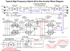

HF hybrid inverter block diagram.png

I found several damaged IGBT's in the PWM output section, again with thanks to RCinFL who helped with the diagnosis. However, there is visible damage in another part of the circuit board which is in the PWM circuit as far as I can tell, but seems like it shouldn't have been damaged. I say 'seems like' because I don't know exactly how the circuit works.

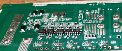
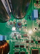
The damage is in an area of the board that contains a TI 2845B current mode PWM controller. Here is the datasheet. The specific damage is that the board swelled, breaking at least one via and popping off two surface mount resistors. There may be other damage. Here is a picture after my repair to the damaged via (the PWM IC is on the opposite side):
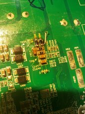

20240307_141514_resized.jpg

My first question is how this part of the circuit could have been damaged. It seems like it is upstream of the Opto-PWM gate drivers and they seem ok (there are a total of 12, one for each IGBT, and they are not shorted from the input side to the output side).

The next question is if anyone has a typical schematic that would show how a PWM controller would be configured with Opto-PWM gate drivers? I've looked for application guides on this and similar PWM controllers with no luck.

The last question has to do with identifying two components on the board so I can test them and/or replace. They are the two 4 terminal components labeled Q41 and Q42 and are right next to the PWM controller.
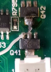
Q41 and 42.jpg

It seems like they would be transistors, but from the markings and the dimensions of the part, I'm not sure. The markings on one (Q41) says M 304 Y, but the closest I can find on google is a PBSS304PZ. Datasheet here. The markings on the other part in question (Q42) are N 30? Y where the ? is unreadable). Could it be that one is a PNP and the other NPN? I'm confused because the datasheet for the PBSS304PZ shows that the part measures 6.7 x 7.3 mm, whereas the part on the board measure 4.3 x 5.4 mm and I can't find anything closer.

Thanks for any suggestions!
 
When output IGBT's get blown out they often present high AC voltage to gate drive circuitry to IGBT's.

This often blows out the opto-isolated driver that drive the IGBT gate. Look for 8-pin IC's on backside of PCB.
The series resistor to IGBT gate is also often smoked.

Sometimes it damages the isolated 15vdc supply that provides the gate drive power.

IGBT PCB backside Opto isolators.jpg

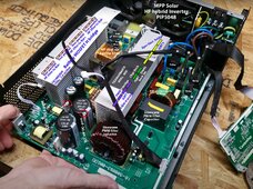
The picture below is MPP inverter but all the low cost HF inverters PCB component placements are pretty much the same.
The low DC voltage supplies are in the lower left-hand corner. Opto-isolator drivers on opposite side of PCB in that area.
HF PIP5048 board with lables small.jpg
 
Last edited:
When output IGBT's get blown out they often present high AC voltage to gate drive circuitry to IGBT's
I found two drivers (out of 12) that are shorted. They are shorted from Vcc to Vee. I have to do some more checking, but I'm hoping that is also why the two 5 ohm resistors overheated and lifted from the board.
Look for 8-pin IC's on backside of PCB
The only 8 pin IC in the area is a TI TL2845B PWM controller. The thing I don't understand about this is that it is not driving the gate drivers, it is actually connected to the output side of the gate drivers. The MCU appears to be driving the gate drivers. So what would the PWM controller possibly do?
Sometimes it damages the isolated 15vdc supply that provides the gate drive power.
I think (hope) the fact that the output side of the drivers is shorted explains the lifted resistors. But since after my first attempted repair, where I only resoldered those two resistors, they lifted again after power was applied indicates that the 15V supply is still good.

My last question is if I spend the $150 or so on parts to fix the known issues (each H bridge module is $65) but I overlook some other bad component or connection, what is the likelihood of blowing out those H bridges again (the first time was bc of me stupidly shorting the battery terminals)? Let's say one of the gate drivers doesn't work for whatever reason, could that destroy the H bridge?
 
The gates, and emitters of IGBT are jacked way up voltage, 15vdc above HV DC level. This absolutely requires isolated gate 12-15 volt gate drivers.

Some gate driver circuits have high voltage processing design and use a boot-strapped supply capacitor to power the upper driver. The supply capacitor is recharged to +12-15v every time the bottom MOSFET is pulled to negative supply. They usually don't use boot-strap drivers for IGBT's because their collector saturates at 1.5 to 2 volts above their emitter, taking too much voltage off the bootstrapping supply voltage.

The TL2828458 is a driver but does not have bootstrapping. The input logic control to TL28284 has to have the supply isolation to high voltage IGBT supply. The whole TL28284 is jacked up in the air (HVDC-wise) as IGBT is switched so the TI drivers input clocking has to have the isolation.

There is also a totally isolated 15vdc supply to power the TI driver chip. The 15vdc supply gets jacked up the air when the upper IGBT conducts.

If when IGBT gets damaged, if its failure creates high voltage to be created between its gate and emitter, it will blow out the driver. The fact that the IGBT series gate resistor was cooked says there was high current pushed through it to gate driver, likely meaning 15v gate driver is also toast.
 
Last edited:
Some gate driver circuits have high voltage processing design and use a boot-strapped supply capacitor to power the upper driver.
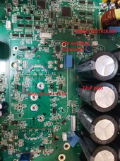
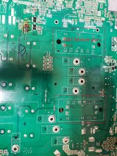
The only caps in the area are two 0.22uF 630V. Do you think the would be for boot strapping? Here are pics of both sides of the board:


20240326_151611_annotated.jpg

20240326_151715_annotated.jpg

The input logic control to TL28284 has to have the supply isolation to high voltage IGBT supply. The whole TL28284 is jacked up in the air (HVDC-wise) as IGBT is switched so the TI drivers input clocking has to have the isolation.
OK, I'll look for another opto isolator going to the TL2845B.

There is also a totally isolated 15vdc supply to power the TI driver chip. The 15vdc supply gets jacked up the air when the upper IGBT conducts.
The 15V comes from another board with a bunch of switching power supplies. I noted the connector in one of the photos. But instead of 15V and ground, the pins are 15V and Bus(-). Does the Bus (-) act as ground???

The fact that the IGBT series gate resistor was cooked
Those two resistors that were cooked (but still measure correct resistance) are in parallel so 2.5 ohms total. However, I don't think they are the IGBT gate resistors. Please correct me if I'm wrong, but wouldn't each IGBT need it's own series resistor? I thought they were cooked because the Vcc and Vee of two of the gate drivers are shorted, meaning a lot more current is going through those resistor. But maybe this is all academic....
I will replace the two gate drivers and the two bad bridge modules, but is there anything else I should look for? I hate to spend $150 and ruin the new parts, or something else.

likely meaning 15v gate driver is also toast.
By 15V gate driver, do you mean the opto-gate driver, 2 of which are known shorted,, or the PWM controller (TL2845B)?
 
I keep forgetting we are talking about a PV GT inverter. With a combined module PWM IGBT H-bridge. I don't see any floating drivers in the IGBT Module so there must be something on the main PCB. Follow the gate inputs back from module you should find them.

The TX1 toroid may be the isolating IGBT gate driver transformer feed. It looks like it has multiple coils to drive individual IGBT's. There has to be a driver to the transformer. I am guessing the Q42 and Q41 across from it are the primary side of toroid transformer driver.

There still should be a 15vdc isolated supply for driver which may be the TI part.
 
Last edited:
What are the 6 pin TSSOP's part #'s on top of board. They look like the opto isolators to IGBT gate drive.
 
The collector of Q42 goes to one of the winding terminals (primary?) of TX1. TX1 has two other separate windings. One goes to the Vee pin of U22 and U47, the other goes to U23 and U48 (those last two are the ones that are shorted Vcc to Vee). U22, etc are all UCC23313 gate drivers. BTW, They are not optical as the input stage is an emulated diode. These are the 6 pin TSSOPs you were asking about. Are they the floating drivers? One more thing. All four of those gate drivers go to the same IGBT module. There is no similar circuit for the other IGBT module.

So it appears you are correct that Q41 and 42 drive the transformer. Furthermore, the output of the TI PWM controller goes through a 50 ohm resistor and to the base of Q42.

However, I'm still confused. How can TX1 be the driver for those 4 gates when it is connected to the output side of the isolators?

I believe the 15 V isolated supply comes from the power supply board. There is an opto isolator on that board near the connector.

Here is a better picture of the TX1 area.

20240326_194059.jpg
 
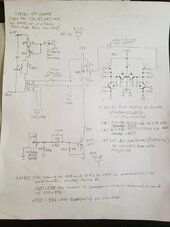
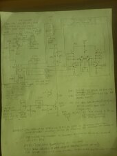
I spent the last two days (maybe 10 hours total) tracing the circuit. It answers a lot of questions I had but raises two others.

Here it is, although there could be a few errors. BTW, I forgot to label the transformer; it is TX1.

Growatt MIN partial schematic gate drivers.jpg

My main questions are regarding the two transistors driving the transformer:

1. Is it more likely that the two 5 ohm resistors are connected to the common emitter junction instead of as I have drawn? This is the area of the board that expanded due to heat and the via connection between sides broke so even though I think it is right, I can't be sure.
2. I'm not sure if the transistors are actually NPN and PNP as I have drawn since I couldn't find the parts based on the markings. The emitters and bases are definitely connected together. Knowing that, is there any other configuration that would make sense?

Most of the time was spent trying to figure out the isolated 15V supply. I couldn't see how the supply on the main board with the small transformer (TX1) was connected to all of the gate drivers. It turns out there is another 15V supply on the separate power supply board! I also figured out why I was confused about the wiring of the gate drivers. I thought the 15V was going to the output side. Well it is in a way since the output pin of that chip is on the same side as the Vcc and Vee pins, but arguably not on the output side of the circuit. Dumb mistake.

So my last question is, now that I am ready to buy the new parts, including two H bridges and two shorted gate drivers, what would happen if I power it up and (a) I still have something wrong with the transistor connections driving TX1, or (b) one of the gate drivers doesn't work, maybe if failed open? Would either of those conditions damage the H bridge? Any way I can test before applying power?
 
Q41 and Q42 are operating in parallel to double their current capability. Check the pin to pin continuity.

The isolation A, B toroid transformer is likely only the 60 Hz of PWM H-bridge switching. The high frequency PWM comes from the HCT244 circuit.
The 60 Hz HV DC polarity flipping is via the 15v drive where the opto-isolator LED is driven by HCT244 for the high frequency PWM switching, creating a logical 'AND' function. The high frequency PWM repeats for each half AC cycle with the isolating toroid does the HV DC polarity flipping.

It could be other way around where the toroid is high freq PWM and HCT244 is 60 Hz switching.

I am guessing the extra two back to back IGBT's in each module holds zero volts for half the 60 Hz frequency period, swapping the zero holding from one PWM module to the other module for each half 60 Hz cycle.

This allows each module side to get a half sinewave PWM switching chopping with the extra IGBT pair in each module alternately hold one module clamped at one side of HV DC for the half cycle.

I see 12 of the 6 pin TSOP opto-isolator chips, six on each of the two modules for IGBT gate input drivers.
 
Last edited:
I am trying to repair a Growatt MIN11400TL-XH-US. I haven't been able to find a schematic for it, but I do have this generic block diagram, courtesy of RCinFL.


View attachment 204444

I found several damaged IGBT's in the PWM output section, again with thanks to RCinFL who helped with the diagnosis. However, there is visible damage in another part of the circuit board which is in the PWM circuit as far as I can tell, but seems like it shouldn't have been damaged. I say 'seems like' because I don't know exactly how the circuit works.

The damage is in an area of the board that contains a TI 2845B current mode PWM controller. Here is the datasheet. The specific damage is that the board swelled, breaking at least one via and popping off two surface mount resistors. There may be other damage. Here is a picture after my repair to the damaged via (the PWM IC is on the opposite side):


View attachment 204438

My first question is how this part of the circuit could have been damaged. It seems like it is upstream of the Opto-PWM gate drivers and they seem ok (there are a total of 12, one for each IGBT, and they are not shorted from the input side to the output side).

The next question is if anyone has a typical schematic that would show how a PWM controller would be configured with Opto-PWM gate drivers? I've looked for application guides on this and similar PWM controllers with no luck.

The last question has to do with identifying two components on the board so I can test them and/or replace. They are the two 4 terminal components labeled Q41 and Q42 and are right next to the PWM controller.

View attachment 204442

It seems like they would be transistors, but from the markings and the dimensions of the part, I'm not sure. The markings on one (Q41) says M 304 Y, but the closest I can find on google is a PBSS304PZ. Datasheet here. The markings on the other part in question (Q42) are N 30? Y where the ? is unreadable). Could it be that one is a PNP and the other NPN? I'm confused because the datasheet for the PBSS304PZ shows that the part measures 6.7 x 7.3 mm, whereas the part on the board measure 4.3 x 5.4 mm and I can't find anything closer.

Thanks for any suggestions!
These are indeed transistors, the text printed on them looks like manufacturers ID codes rather than product IDs... In the picture it looks like a solder bridge is shorting the two parts together so this could be the reason for the blown resistors R885 and R886. you could use a DMM to check for the B-E and B-C diode junction diodes, if you only find 1 junction then they are probably mosfets.
 
Q41 and Q42 are operating in parallel to double their current capability. Check the pin to pin continuity
That's what I would have thought, but is that possible the way they are connected? The bases of each are definitely connected together, as are the emitters. I can see that visibly in the traces and verified with DMM. And the collectors are definitely connected as shown. The only uncertainty is whether the 5 ohm resistors should connect to the common emitter junction (for faster turn off?), or as shown to the collector of Q42. Maybe it would work either way?? I googled how transistors would be connected in parallel, but couldn't find anything that matches what I know for certain about the circuit.
The isolation A, B toroid transformer is likely only the 60 Hz of PWM H-bridge switching. The high frequency PWM comes from the HCT244 circuit.
The 60 Hz HV DC polarity flipping is via the 15v drive where the opto-isolator LED is driven by HCT244 for the high frequency PWM switching, creating a logical 'AND' function. The high frequency PWM repeats for each half AC cycle with the isolating toroid does the HV DC polarity flipping.

It could be other way around where the toroid is high freq PWM and HCT244 is 60 Hz switching.
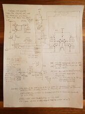
I revised the schematic to show how the different gate drivers are powered. Interestingly, the TX1 transformer is only driving gate drivers for one of the H bridges (4 of them on M2 as shown). The gate drivers for M1 are all powered by the separate power supply (which also powers the two remaining gate drivers for M2).

Growatt MIN partial schematic gate drivers Rev A.jpg

I am guessing the extra two back to back IGBT's in each module holds zero volts for half the 60 Hz frequency period, swapping the zero holding from one PWM module to the other module for each half 60 Hz cycle.
Does seeing how the different gate drivers are powered give any clue to this?

I see 12 of the 6 pin TSOP opto-isolator chips, six on each of the two modules for IGBT gate input drivers.
Yes, there are 12, 6 for each H bridge. There are 4 other identical chips, but they are in the MPPT section.
 
These are indeed transistors, the text printed on them looks like manufacturers ID codes rather than product IDs... In the picture it looks like a solder bridge is shorting the two parts together so this could be the reason for the blown resistors R885 and R886. you could use a DMM to check for the B-E and B-C diode junction diodes, if you only find 1 junction then they are probably mosfets.
Sorry for the picture quality, but in person I can verify there is no solder bridge (also checked with DMM). I'm 95% certain that the damage was caused by the shorted gate drivers (caused by the shorted/open IGBT's).

I tested the B-E and B-C junctions with the following results (essentially the same for both Q41 and Q42):

B-E .6V on diode function
B-C .1M on resistance function
E-B .6V
C-B .1M

Does this help? BTW, this was all done in circuit.

I googled mosfets in SOT89 package (based on dimensions of the chip) and couldn't find anything. All I could find that seemed close and had a 304 in the part number was the BJT per the attached datasheet (available in a complimentary version).
 

Attachments

  • Possible 304 transistor PBSS304PZ.pdf
    301.7 KB · Views: 2
From your measurements they do look to be BJT's rather than FET's,

The series circuit you have for these doesn't make sense unless you consider that due to manufacturing process PNP and NPN transistors usually have different pin configurations (base, emitter and collector are usually on different pins). In which case the circuit could be setup as a sziklai pair as shown below.. (see google)

sziklai pair
 
Last edited:
From your measurements they do look to be BJT's rather than FET's,

The series circuit you have for these doesn't make sense unless you consider that due to manufacturing process PNP and NPN transistors usually have different pin configurations (base, emitter and collector are usually on different pins). In which case the circuit could be setup as a sziklai pair as shown below.. (see google)

sziklai pair
If it is true that they are BJT I think chances are good that they are the transistors in the datasheet I uploaded. Per both datasheets, the PNP and NPN have identical pinouts.

If thats the case, then it means my diagram is correct, with the possible exception of where the 5 ohm resistors go. I can't find it now, but I saw a PNP-NPN circuit on line which is the same as mine with the exception that the load is connected to the common emitter junction. They said that adding the PNP, which replaced a resistor, helped the circuit turn off faster. I don't think they mentioned the application.

Now that I have a better idea of the circuit, I think I will apply 15v again and try to get better measurements and wave forms. I may also try switching the connection of the resistors to the emitters to see if there is any difference. I will remove the two shorted gate drivers first of course. Any other suggestions?
The BJT's wont function in the circuit the way it is drawn. The NPN will prevent the PNP from transisting and the PNP will stop the NPN from transisting. Both transistors are in common collector mode, which makes the C-E conduction of both devices mutually exclusive). Since the emitters are not connected there will be no current flow (except for neglible leakage current).

FYI: Manufacturers rarely put the part code on the SOT23 or smaller packages (because of legibility issues). Usually they put a batch/date code.
so N 304 Y and M 304 Y are probably from two batches assembled on the same day. batch N followed by batch M on day 304 of year Y.
(That's just my guess from the numbers).
 
The BJT's wont function in the circuit the way it is drawn. The NPN will prevent the PNP from transisting and the PNP will stop the NPN from transisting. Both transistors are in common collector mode, which makes the C-E conduction of both devices mutually exclusive)

So if it won't work as drawn, would it work if they were both PNP or both NPN? If so, what would be the purpose of having two identical transistors in series?

Since the emitters are not connected there will be no current flow (except for neglible leakage current).
Not sure what you mean by if the emitters are not connected. Do you mean to a load?

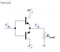
BTW, I found the circuit with the PNP and NPN connected in series with the load connected to the common emitter junction. Here is a screen shot and a Link to the web page that I thought might indicate how Q41 and Q42 should be connected.

1711942064232.png

I didn't get to run the test with 15V power applied to the circuit today, but should have time tomorrow.
 
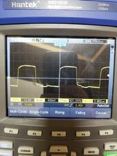
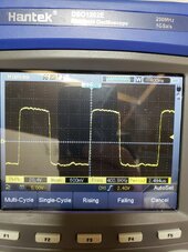
I tested the circuit (as drawn in my sketch, also no H bridge modules installed) with 15V. The wave forms at the transformer were as shown below (400kHz). There was a slight voltage boost across TX1 as would be expected.

Primary of TX1:

TX1 Primary Waveform No H Bridge.jpg


Secondary A of TX1:

TX1 Secondary Waveform No H Bridge.jpg

There was no signal at the gate drivers for some reason. Maybe the rest of the inverter needs to be powered up to enable something.

It seems to be working, but could it be better? I was afraid to relocate the connection at Q42 to make it like the push pull circuit I found on line for fear of damaging something. Not sure what to do next so would appreciate any guidance. Thanks!
 
Sorry for the delayed response/update, I've been out of town. I have updated the 15V isolated supply schematic and am now 98% sure it is correct since it is working (that part of the inverter, anyway).

Growatt schematic 15V supply to gate drivers.jpg

I also ordered and installed the new gate drivers and h-bridges. There was no release of magic smoke on startup, but the inverter still isn't inverting. Crap.

OTHER SYMPTOMS
If the inverter DC (PV input) is off and only powered up by AC, there are no errors, however, the app thinks the AC voltage is 0 and the frequency is 60hz. But when DC is turned on, two faults appear within a few seconds. One indicating AC voltage is above threshold (thinks the voltage is 493 and frequency is 68hz when it is really 250V and 60hz). The other fault is that the inverter thinks the PV voltage is 440V on one input and about 30V on the other three inputs, when in fact it is only 90 volts on one input and 0 volts on the other three.

TROUBLESHOOTING
I rechecked all the gate drivers including the two I replaced and they seem to be good. All the IGBT's and internal diodes of the H-bridges also seem to be good. The gate drivers are getting 20-22V (isolated). I expected something closer to 15V, but that is well within allowable range.

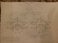
The other attached schematic shows which gate drivers drive which IGBT in the H-bridge. I used that to see which if any of the gate drivers were getting an input signal when powered up. Only 4 of the gate drivers, indicated by an asterisk in the schematic, are getting what may be a startup signal (as shown in the attached video). It seems odd that only one transistor on H bridge module 1 is getting that signal and three transistors on the other H bridge module are getting the same signal.

H bridges layout.jpg
1713756421267.png


About the signal wave form. Channel 1 is yellow, channel 2 is blue. They are set to different voltage scales so that they don't overlap, but you can see that they are identical and in phase. They are measured at the input to the gate driver. There is no corresponding output signal on the output pin. Here is what the datasheet of the gate driver says:

1713755718429.png

One other thing. With the good inverter, when all power is disconnected, it takes about 60 seconds for the inverter to shut down. With this inverter, the shutdown only takes a second or two. The DC voltage on the capacitor bank measures about the same as the input voltage (80-90 volts) so maybe there is a soft short somewhere, but I can't find anything.

I don't know what else to check. Any ideas of things that might have been damaged when the DC input (i.e. battery terminals) were shorted? I swapped the comm board from the good inverter and got the same errors, so it must be something on the main board.
 
Back
Top