diy solar

diy solar

Warpverter

Nobodybusiness

Collecting the leftovers of the Great Sky Reactor.
Joined
Dec 19, 2021
Messages
3,898
Location
Earth
Because fifteen cells stack as 5 x 3 very neatly, and sixteen cells stack together as a much less convenient shape at 8 x 2

I design and build all my own solar electronics, and can have any system voltage I want.
So I decided that thirty cells at around 3.3v nominal = 100 volts.

Dare to be different !!!
Are you using some type of High voltage DC input inverter?
 
Are you leveraging existing High DC input designs or just coming up with your own?

What are you running with a 5kw inverter?
Its completely my own unique design, pure sine wave, but NOT using the usual pulse width modulation.
Load is just normal domestic loads at my home.
Its been functioning without a single problem for almost six years.
Several other people over at The Back Shed forum have also successfully built these. All are in the 5Kw to 7Kw class so far.
There are about twenty Warpverters now in successful operation around the world that I know of.

They can be built for any input or output voltage 50Hz or 60Hz and any power level, there is no practical upper power limit.
Below about 4Kw to 5Kw, conventional pwm transformer inverter would be cheaper to build.
But at higher power levels the Warpverter has far fewer problems, is easier to get going, will be more robust electrically, and have better reliability.

Idling power and efficiency pretty much the same as pwm.
 
Last edited:
Its completely my own unique design, pure sine wave, but NOT using the usual pulse width modulation.
Load is just normal domestic loads at my home.
Its been functioning without a single problem for almost six years.
Several other people over at The Back Shed forum have also successfully built these. All are in the 5Kw to 7Kw class so far.
There are about twenty Warpverters now in successful operation around the world that I know of.

They can be built for any input or output voltage 50Hz or 60Hz and any power level, there is no practical upper power limit.
Below about 4Kw to 5Kw, conventional pwm transformer inverter would be cheaper to build.
But at higher power levels the Warpverter has far fewer problems, is easier to get going, will be more robust electrically, and have better reliability.

Idling power and efficiency pretty much the same as pwm.
That’s very interesting.

Do you have any firmware running?

Data screens?

How did you overcome all the issue that commercial inverters have to deal with?

If you don’t use PWM for wave formation what do you use?

I’m not doubting you, I’m just trying to figure out if there is a way to build one sufficiently robust then why buy them?
 
Last edited:
It does not use pwm, but combines the output of four low frequency square wave inverters.
Each of these inverters has an output transformer that has a different secondary voltage. The four secondaries are connected in series to directly generate an analog ac sine wave. Its rather like direct digital to analog conversion at hundreds of volts and thousands of watts.
Each square wave inverter has potentially three output states +ve, zero, and -ve. There are four inverters (four bits).

As you will know, four bits of binary can only produce 2 x 2 x 2 x 2 = 16 output voltage levels.
Four bits of "trinary" can produce 3 x 3 x 3 x 3 = 81 output voltage levels.
That is an 81 step peak to peak sine wave, forty steps up, zero, and forty steps down.

I developed this gradually myself over many years. The original prototypes all used various microcontrollers to generate the required switching waveforms. But I gradually simplified it down to be an all hardware design (no software crashes !)
This makes it a lot easier to understand and repair for people that are not software geniuses.

At least two other software guys have come up with firmware that duplicates my hardware design using a Nano microcontroller.
There are now three different Warpverter driver boards available to do all of this from three different people. All are 100% compatible with identical plugs and identical functionality. Its all free and completely open source if you wish to build one yourself.

No data screens or firmware. Its a basic bare bones inverter, dc in, ac out. No problem adding a second microcontroller for purely monitoring, alarms, logging or control. That would be quite independent of the basic inverter function, so you can add whatever you want yourself.

As a retired professional power electronics design engineer, its been a bit of a part time hobby. Having designed mass produced commercial inverters and uninterruptible power supplies, overcoming the technical problems is what I do.

The only problem with it is its not commercially viable, its too expensive to build compared to pwm. So its only value is as a home project where you wind your own transformers and use recycled parts.
The biggest advantage is all the switching is done at at a very low frequency, so the circuit layout is far less critical than high frequency pwm, where it becomes increasingly difficult to successfully parallel multiple devices for very high power.

This is what the secondary voltages look like. All waveforms shown with the same oscilloscope settings.
 

Attachments

  • composite steps.jpg
    composite steps.jpg
    624.5 KB · Views: 64
Should have massive surge capability, up to maybe 20x if enough FETs.
 
It certainly does have massive surge capability, fully protected on the ac side with just a normal C curve thermal/magnetic circuit breaker.
Its also fully bi directional. Really nasty highly reactive loads can bounce out of phase current right back onto the dc bus.

All the Warpverters now running have fired up and run first go, and been completely trouble free and essentially bullet proof.

Only one guy had any problems, and that was due to him using the wrong crystal frequency.
He fitted a 32.768 Khz watch crystal, instead of 3.2768 Mhz.
His Warpverter tried to run at 0.5Hz instead of 50Hz. As he did not own an oscilloscope at the time, that problem took a while to figure out.
But with the right crystal it all worked, and he is now very happy with it.
 
Last edited:
Transformer saturation (zero volts across them, except for IR drop) should have been the first clue.

Funny shape of the crystal can, the second.

I once worked on a product (Palm Pilot VII) that specified a 10 ppm 32 kHz crystal. They were hard to come by (mostly 30 ppm) and constrained volume. If they had just designed it for 32.768, those were available everywhere. Maybe could have functioned with standard watch crystal, but radio certainly wouldn't.
 
One other very unusual feature of the Warpverter is that there is no voltage feedback from the secondary windings required.
The output voltage is regulated using voltage and (optionally) current feed forward instead of feedback.
I have never seen another inverter do that !!!

But this is interesting. It responds much faster to step load changes than feedback ever could.
And it can be tweaked so that the ac output voltage can decrease, stay the same, or increase under increasing load.

Its possible to over compensate for having a very long wiring run between the inverter and load, so that the voltage at the load is well regulated in spite of a large and varying voltage drop in the wiring.
Its all jolly good fun, and a really interesting project.
Googling "Warpverter" will turn up a few articles, threads, and pictures.
 
Transformer saturation (zero volts across them, except for IR drop) should have been the first clue.

Funny shape of the crystal can, the second.

I once worked on a product (Palm Pilot VII) that specified a 10 ppm 32 kHz crystal. They were hard to come by (mostly 30 ppm) and constrained volume. If they had just designed it for 32.768, those were available everywhere. Maybe could have functioned with standard watch crystal, but radio certainly wouldn't.
Most of those 32 Khz "crystals" are not real quartz crystals, but a kind of piezo ceramic tuning fork like device.

Even a two dollar Chinese clock will easily out perform the very best and most expensive marine navigation chronometer of a hundred years ago.
 
It does not use pwm, but combines the output of four low frequency square wave inverters.
Each of these inverters has an output transformer that has a different secondary voltage. The four secondaries are connected in series to directly generate an analog ac sine wave. Its rather like direct digital to analog conversion at hundreds of volts and thousands of watts.
Each square wave inverter has potentially three output states +ve, zero, and -ve. There are four inverters (four bits).

As you will know, four bits of binary can only produce 2 x 2 x 2 x 2 = 16 output voltage levels.
Four bits of "trinary" can produce 3 x 3 x 3 x 3 = 81 output voltage levels.
That is an 81 step peak to peak sine wave, forty steps up, zero, and forty steps down.

I developed this gradually myself over many years. The original prototypes all used various microcontrollers to generate the required switching waveforms. But I gradually simplified it down to be an all hardware design (no software crashes !)
This makes it a lot easier to understand and repair for people that are not software geniuses.

At least two other software guys have come up with firmware that duplicates my hardware design using a Nano microcontroller.
There are now three different Warpverter driver boards available to do all of this from three different people. All are 100% compatible with identical plugs and identical functionality. Its all free and completely open source if you wish to build one yourself.

No data screens or firmware. Its a basic bare bones inverter, dc in, ac out. No problem adding a second microcontroller for purely monitoring, alarms, logging or control. That would be quite independent of the basic inverter function, so you can add whatever you want yourself.

As a retired professional power electronics design engineer, its been a bit of a part time hobby. Having designed mass produced commercial inverters and uninterruptible power supplies, overcoming the technical problems is what I do.

The only problem with it is its not commercially viable, its too expensive to build compared to pwm. So its only value is as a home project where you wind your own transformers and use recycled parts.
The biggest advantage is all the switching is done at at a very low frequency, so the circuit layout is far less critical than high frequency pwm, where it becomes increasingly difficult to successfully parallel multiple devices for very high power.

This is what the secondary voltages look like. All waveforms shown with the same oscilloscope settings.

Gentlemen, you are hereby ordered to protect this man at all costs!
 
The advantage of this design is low frequency 50/60hz switching. Slow and large power devices like ancient 600A IGBT or BJT power modules can be used which would make this inverter practically indesctructible and have ridiculous surge power capability.
 
The advantage of this design is low frequency 50/60hz switching. Slow and large power devices like ancient 600A IGBT or BJT power modules can be used which would make this inverter practically indesctructible and have ridiculous surge power capability.
That is exactly what I used, four humongous 200 amp IGBT half bridges for the two largest inverters, and individual 50 amp IGBTs for the two smaller inverters. Same identical gate driver boards for each, all mounted on one large isolated heat sink.
Very simple mechanically, and quite compact.
After six years of thinking about it, I would not do it any differently today, if I decided to start building another one for some reason.

If someone needed a 10Kw, 20Kw, or 30Kw inverter, this would scale up really easily.
The transformers would obviously need to be suitably large.
But if you wind your own transformers (from second hand recovered material) it need not be all that expensive for the power levels that would be possible.

Its only if you start winding transformers from all new materials it gets REALLY expensive, and that is what makes it a non starter as a viable commercial enterprise.
 

Attachments

  • 2018-06-26_0001.jpg
    2018-06-26_0001.jpg
    1.7 MB · Views: 67
Last edited:
That is exactly what I used, four humongous 200 amp IGBT half bridges for the two largest inverters, and individual 50 amp IGBTs for the two smaller inverters. Same identical gate driver boards for each, all mounted on one large isolated heat sink.

I was going to say, "But they are in series, carry the same current."
Then, glancing at the schematic, I realized secondary windings are what's in series. Due to turns ratios, primary all carry different current.

You said 3 levels not two; each is MSW not square wave. How do you drive the FETs for shorted winding rather than driven positive or negative polarity of battery? You did indicate FETs happily conduct current either direction when on so I'm guessing two pull downs or pull ups.

You show a dead time of 1 microsecond +/- set by cap across LED of optoisolator. Does an inductive kick appear when FETs are off?

What is no-load current through primaries of transformers?
 
Looks like inverter 1 + 2 is sine wave enough to power dumb loads like motors and heaters.
Can you post links describing your inverter project from the start?
12.JPG
 
I was going to say, "But they are in series, carry the same current."
Then, glancing at the schematic, I realized secondary windings are what's in series. Due to turns ratios, primary all carry different current.

You said 3 levels not two; each is MSW not square wave. How do you drive the FETs for shorted winding rather than driven positive or negative polarity of battery? You did indicate FETs happily conduct current either direction when on so I'm guessing two pull downs or pull ups.

You show a dead time of 1 microsecond +/- set by cap across LED of optoisolator. Does an inductive kick appear when FETs are off?

What is no-load current through primaries of transformers?
There are quite a few hidden features in all of this, that may not be immediately obvious.

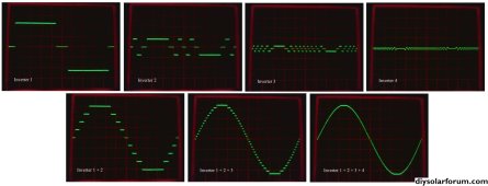
Firstly its not too difficult to see how switching the primaries generate the required three level rectangular voltage waveforms in the secondaries, and how the series connected secondaries all add these together directly, to generate a very low distortion sine wave output voltage.
The measured THD is 0.85% and the strongest harmonic is the third which is down -40db.

What may be less obvious, is that the sine wave current in the secondaries will be continuous and equal in each secondary, and that will be reflected back into the primaries as a constant unbroken sine wave current, regardless of what the mosfets/IGBTs are doing !

Think of these as four square wave voltage transformers in the forward direction, and four sine wave current transformers in the reverse direction.
That is rather odd, but its how this all actually works.

I know this is all a rather difficult concept to get your head around to begin with, but please try to bear with me....

Because of this continuous sinusoidal primary current, the zero volt output state requires a shorted out primary winding, because current must continue to flow when a particular transformer is outputting zero volts.

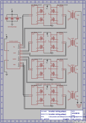
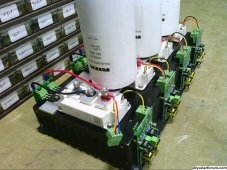
Each primary is driven by four IGBTs (or sometimes mosfets) in a conventional hard switched bridge configuration. Diagonal IGBTs are turned on to switch battery voltage direct across the primary in the usual way.
To short out the primary, during the zero volt part of the waveform, we can turn on either both lower IGBTs together, OR both upper IGBTs together.
It does not really matter, the result will be the same either way.

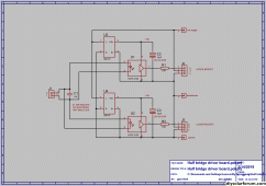
The half bridge driver boards each drive one upper and one lower IGBT on one side of each bridge. Opto isolators are used, but the opto isolator LEDs are connected in inverse parallel, so its impossible for both opto isolators to be on together. This feature reliably prevents any shoot through problem, where upper and lower IGBT might conduct simultaneously. By adding some capacitance across the opto LEDs, that generates reliable and symmetrical dead time.

All of these features combine to make for a very robust switching bridge that is extremely immune from noise, or corrupted data that may occur during power up or power down, or brownout. Its the secret to designing very robust inverters that do not randomly blow up !

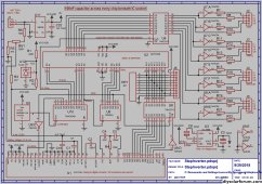
Data comes from the control board over a balanced low impedance twisted pair, that is opto isolated at the far end. This provides extremely high noise immunity and the twisted pairs can be made quite long without any worries about picking up noise. That can be rather important at very high power levels.

One data bit controls one side of the bridge. Logic 0 is lower IGBT on, Logic 1 is upper IGBT on. Always one or the other is on, except during dead time. There are four possible logic drive states to each bridge 00, 01, 10, and 11. All are safe in the respect that corrupted data might put a momentary kink in the sine wave, but it cannot blow anything up.

So basically the whole of the four power switching stages are very well protected from noise or being driven with scrambled or corrupt data. This goes a very long way to designing a very reliable bullet proof inverter.

As far as no load idling current goes, my own 5Kw inverter draws 32 watts of total dc idling power. About five watts of that is for the control board, and the rest is just mostly transformer magnetizing current. Other Warpverters vary a bit, I think the record so far is about 20 watts of idling power for a 7Kw inverter. There is a bit of luck involved that concerns the quality of the core material used in the transformers. Some material is excellent, and some less so....
More on designing the transformers later.
 
Last edited:
Back
Top