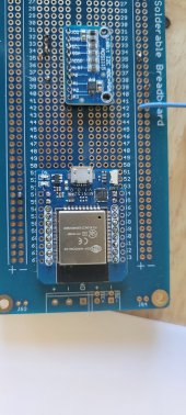
SO I am looking to build BMS sensing modules on a single board I have prototypes but would like to get custom PCB's for my project. The problem is I really do not want to learn how to CAD design a PCB. Does anybody have any knowledge they can help me with. Obviously I can provide a sketch of what I need.
Thanks!
Give
KiCad a try! It's really not very complicated and fun to use!
I've uploaded the gerber files to
JLCPCB and they charge you $2 for 1&2 layer boards (100x100mm) with drilling, solder mask, silkscreen, testing, etc. You have to buy 5 minimum, so it will be $10 total plus shipping (DHL express $16.25). For new customers they gave a $5 bonus. They even offer cheap option for PCB's with already soldered SMD components when you use components from their component repository (but I never tried this). This should not be advertisement, it's just my experience with them.
I've done this a couple of times and I'm REALLY IMPRESSED about the quality and how fast it was produced (24h) and shipped (8 days). You can (more or less) follow online how your PCB runs in detail through the production line.
I will never try to build a PCB by myself again (beside initial breadboard tests).
Here is an example of one of my orders:
MI: 2022-04-12 20:44:48
Drilling: 2022-04-12 22:16:03
Copper Deposition: 2022-04-12 22:22:02
Image the outer layers: 2022-04-12 22:56:03
Pattern Plating: 2022-04-13 01:36:55
Automatic Optical Inspection(AOI): 2022-04-13 01:41:10
Solder Mask: 2022-04-13 03:43:14
Silkscreen: 2022-04-13 07:12:12
Hot Air Solder Leveling(HASL): 2022-04-13 07:33:02
Electrical Test: 2022-04-13 08:57:52
Profiling,V-cut scoring: 2022-04-13 13:38:23
Final inspection: 2022-04-13 15:56:21
Delivery