diy solar

diy solar

I want to make my own BMS

I continue to dream of a really well considered DIY BMS with open source code......

OP: Is this what you are thinking on this one?
I have the skills and physical resources to make my own - but lack the time resources to go end-to-end.

The most interesting system I have seen so far is Batrium. They have a slick modular approach and seemingly decent software to program and monitor. They do not, however, cover all the things I would like to see covered though. Great start and a decent price for what you get.
The myriad of random Chinese offerings are super sketchy most of the time.

My Chargery system is NOT something I will count on. It is a toy.
 
I am not thinking in an open source project per se. I am thinking in a project for myself open for the comunity. After I finish it I do not mind keeping the support or modifications, so in the end it would be an open source project. I also have some time problems but this project seems rather easy.
 
Maybe I am confusing them with SSRs?

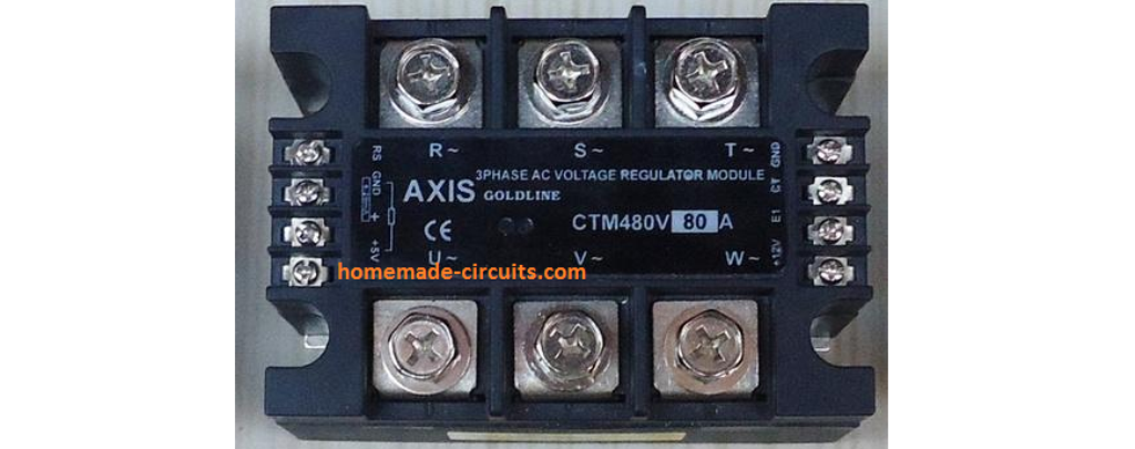
DC SSR's are just MOSFETs with some control scheme. It is possible that the control circuit on a specific unit could latch for a variety of reasons. My first few guesses would be related to poor design.

For high-current systems like large LiFePO4 banks - it is definitely worth the effort to get your control circuits dialed in really well and consider the consequences of various failure modes.


I am not thinking in an open source project per se. I am thinking in a project for myself open for the comunity. After I finish it I do not mind keeping the support or modifications, so in the end it would be an open source project. I also have some time problems but this project seems rather easy.
Conceptually it is easy, but be careful not to underestimate the gritty details.
For me, the slowest part is the firmware and software that would be needed to achieve my personal goals. The concept evaluation hardware, I could design the schematic, layout a PCB, and get it to fab fairly quick.

Designing it in a way that facilitates the actual end-user experience is another pass through the design system. That is where enclosures, connectors, external communication, etc come into play which is very different than the solving the core electronics functionality - making it practical in real life scenarios.
 
DC SSR's are just MOSFETs with some control scheme. It is possible that the control circuit on a specific unit could latch for a variety of reasons. My first few guesses would be related to poor design.

For high-current systems like large LiFePO4 banks - it is definitely worth the effort to get your control circuits dialed in really well and consider the consequences of various failure modes.


Conceptually it is easy, but be careful not to underestimate the gritty details.
For me, the slowest part is the firmware and software that would be needed to achieve my personal goals. The concept evaluation hardware, I could design the schematic, layout a PCB, and get it to fab fairly quick.

Designing it in a way that facilitates the actual end-user experience is another pass through the design system. That is where enclosures, connectors, external communication, etc come into play which is very different than the solving the core electronics functionality - making it practical in real life scenarios.
Firmware (only the BMS protection and comunication) I do not expect more than one day. I have been 8 years doing exactly this, taking a concept of an electronic design and making it true for the customer. The only part I expect time is testing where I need to setup the bench, hook multimeters oscilloscope....
 
Firmware (only the BMS protection and comunication) I do not expect more than one day. I have been 8 years doing exactly this, taking a concept of an electronic design and making it true for the customer. The only part I expect time is testing where I need to setup the bench, hook multimeters oscilloscope....
If that is true....hats off.
Personally, in my 15 years of professional design, engineering, and manufacturing, I have never worked with person or a company that can deliver safe and functional firmware in the range of a BMS system even remotely that fast. At least not something I would count on for anything.

Look forward to seeing where this goes.....
 
DC SSR's are just MOSFETs with some control scheme.
I guess my bias come from the EV segment. I realize the loads are significantly different.
I have 3 spare Tyco contactors so when those are toast, I will keep an open mind the next time I need to buy a shut off device.
 
I guess my bias come from the EV segment. I have 3 spare Tyco contactors so I will keep an open mind the next time I need a shut off.
In EV's - those big contactors are a great idea since the pack voltage is really dangerous and (guessing by law) they need to absolutely guarantee a physical disconnect without any reliance on control circuits and MOSFETs.

They must be fairly expensive at new cost, no?
 
With single wire for charging and discharging you cannot control the current direction with mechanical relays. The only way is with fets. Normally they are set like in the next diagram.

main-qimg-106c212265273097e4d22d52897d9837.webp


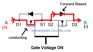
During normal operation both conduct current. For example if you want to allow current only from the left to the right, you keep left fet on and right fet off. The right fet will conduct through the body diode current from left to right and will block from right to left. The drawback of this scheme is the power disipation because the right fet will dissipate P=Ix0.8v but it is the standard way in BMS. As this is in faulty sittuations this shouldn´t happend a lot.
Welcome to the forum! I wish you success with your design. I've seen a number of people who stated they wanted to build their own BMS on this forum. Either they gave up or they stopped posting. The design and build is not as easy as you portray. For example, your description of the mosfet circuit is incorrect. The body diode should never conduct. The die would have a meltdown! You need to come up with a better design.
 
Welcome to the forum! I wish you success with your design. I've seen a number of people who stated they wanted to build their own BMS on this forum. Either they gave up or they stopped posting. The design and build is not as easy as you portray. For example, your description of the mosfet circuit is incorrect. The body diode should never conduct. The die would have a meltdown! You need to come up with a better design.
Hi @Cal , thank you for your welcome!

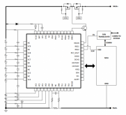
The body diode of a mosfet has the same current capability as in its ON state. If a mosfet can conduct 100A, it will be able to do it also through the body diode. The main difference is that you will have 0.8V voltage drop so power dissipated P=0.8xI and current should be limited. This is not my invention. This is one of the ways done in in commercial products and you can see it in many many designs.

This is just an example:

test.PNG
 
Last edited:
Mosfets are bipolar. The body diode will not conduct.

Also, the diagram you show isn't really the best design. In typical applications load current might be 5 times greater than charging current. That means charging current fet on resistance doesn't have to be as large as the load fet on resistance. But since they are back to back, the two fets must have equal on resistance. I suggest you have a separate charge and discharge path.

Separate current paths
I do not want to go in deep technical discussion but talking about NMos in this case, they are bidirectional in ON state and unidirectional in OFF state. That is why you need to use 2 mosfets with the body diode in oposition to totally disconect the battery, because body diode conducts. In the case it would not conduct you would only need 1 mosfet. It is how DC SSR are built and they need to use 2 mosfets.

The situation where one mosfet is ON and the other one is OFF conducting thtough the internal diode is only during abnormal situation.

Charge can be disabled during low temperature and discharge stays enabled to activate heaters or keep some of the basic electronics ON.
Discharge can be disabled when battery is too low and you want to charge the battery momentarily until you rise the battery state of charge some amount, avoiding loads discharging the battery.

If charging is disabled because, maybe low tempearture, and you plan to discharge high current you might have problems.

During normal operation both Mosfets are enable and conducting bidirectionally.

As I said, separating current paths is not an option for me as I have an all in one charger/inverter as many people.
 
Last edited:
Welcome to the forum! I wish you success with your design. I've seen a number of people who stated they wanted to build their own BMS on this forum. Either they gave up or they stopped posting. The design and build is not as easy as you portray. For example, your description of the mosfet circuit is incorrect. The body diode should never conduct. The die would have a meltdown! You need to come up with a better design.
Not sure what you are talking about. This diagram of back-to-back FETs is really typical for bi-directional control. Pretty much exactly what a basic BMS needs.

Are you referring to a 2-port BMS concept with separate charge/discharge? I believe the OP already said that is not part of the plan.
 
Of course, Mosfets when they are in OFF state conducting though the body diode will disipate lots of power but this only happens during abnormal situation. The idea is to recover back to normal situation ASAP.
 
What do you mean by an abnormal situation duration? Milliseconds??? or microseconds?
 
It is not about the time, it is about the frequency of the situation.

To disable charge I could imagine 2 abonormal situations:

A situation where your battery is under 0 celsius that can happen 4 times per year (if it happens more it would be better to review the battery enviroment). You will be able to use your battery until you fix the temperature of them.

Something failed and your battery got overcharged because voltage is rising too much. Your battery will be able to discharge to safe voltages but not charged more until the right voltage is restored. This should never happend.

The abnormal situation duration is not relevant as your focus is to protect and save the battery, not worry about some watts losts because of the voltage drop during this situation.
 
And I will say again, separated paths is obviously better but not every system allows it. I do not see merged paths as a problem as these situations would only happen hardly ever and drawbacks are not big enough to worry.
 
I just found a website that explains this mosfet configutation much better than me:
BPS-Configuration-%E2%80%93-Back-to-Back-Connected-using-N-MOSFETs.png

 
Back
Top