diy solar

diy solar

I want to make my own BMS

Your diagram looks good. Doesn't look like too much design work. It will be interesting seeing how the disconnect fets work. That's your biggest unknown. How much power do they dissipate during a fault condition. That determines how many fets in parallel you need. I wouldn't put those fets on your primary circuit board. That would be too restrictive.

When are you starting?
 
I Like the approach, should be a fairly flexible design using the BQ76952.
I have mused over many different designs, all with their pros and cons.

PCB Design:
The BQ chip & its reference does address most of the grunt work for implementing the design, the schematic and pcb would be nice to layout to make it customizable for different series layouts of the cells. So the one design can be used for different sized packs.
Id like to see one small main board with MCU, BQ chip, low current balancing, temp sensors, small gauge wire connections, Voltage supply & charge pump.
And then a daughter board with the Fets on it that could be designed in 2-4 different sizes to accommodate different current requirements.
The shunt is tricky, it kind of needs to be sized for the application which would lead it to be on the daughter board, but it needs to be carefully integrated on the PCB with the mcu to maintain much SOC accuracy.
Using common source/drain mosfets is pretty much the best way, and the only way if you want single connection but making it charge only etc.
There will be some loss on the body diode during this operation. But the battery often leaves the charge or discharge only condition quickly, and there are few times where you would need the body diode conducting, the bms fets should never be switched off in an ideal scenario anyway. Your inverter should stop charging before max voltage and stop discharging before max discharge anyway.

Balancing:
For small packs <1kwh, ~100ma balancing is often sufficient, low powered and small enough to include on the main board PCB (With a temp sense for derating)
For large packs, even a small balance current can be sufficient if you are clever in software.
Lets look at top balancing, as you are charging, you log the cells voltage and accumulated current / MAH. When you hit your end point in charge (low current cv) say your pack looks like C1: 4.17 C2: 4.11 C3: 4.10. You look back in the log and see how many MAH it took for C1 to go from 4.10 to 4.17, you then run the balance mosfets until you have removed that many Mah from c1. In theory it should now be at 4.1.
Top balancing does this by just running the balance mosfets until the voltage is even. The advantage of the predictive approach is that the battery doesnt have to remain at the balance voltage while the fets are running, only for the few mins for the voltage to settle and be measured. When the pack next reaches its balance voltage you reassess and rerun your algorithm.
The other way is you could look at the curve for a given chemistry and the pack AH and predict a coefficient, eg 1mv balance error = .4ah to be discharged.

Active balancing:
For large packs that need a larger amount of balancing in perpetuity it is worth active balancing, mostly so as a designer you dont have to deal with as much heat dissipation on the pcb, but the efficiency and speed advantage is a bonus.
Chips like the ETA3000 work well, but there is a fundamental flaw when using them in large packs. Because each chip only senses its cell and the one higher, and balances to 30mv, you can end up where they are no longer transferring current in this scenario: 4.11 4.13 4.15 4.17 4.19 4.21 4.23. Each chip thinks it is balanced to 20mv, but the pack is well out of balance.
The chips internally are just synchronous buck converters with the feedback point of (vc1+vc2)/2 with a bit of hysteresis and current limiting.
What really needs to happen is that the main MCU synchronizes all of them and tells them what direction to run to balance the whole pack, and to make use of the high accuracy ADC in the BQ chip to shuttle charge to end up with an accurate final balance. This could also run when the pack isn't just at balance voltage.

Software:
For the Coms, bluetooth is only useful if there's a companion app that can be used to see and set parameters for mobile/portable applications
Wifi would be great, would be useful to be able to transmit Voltages, currents, SOC, Balance accumulation, ETC over mqtt. This can permit logging with Emoncms, or grafana/influx. Or integration in to other systems.
A specified UART protocol could be useful.
Most flexible would be making the main mcu arduino compatible, opens up tweaking the code to customise the operation to a wider audience.
Id likely try use an ESP32 for the Main mcu, which can easily do bluetooth & wifi if needed, and should be more than fast enough to interface with the BQ chip.
It would also be needed to have some way to edit the calibration values for cell voltage measurements.

I see little need for the SOC Mcu or the balance mcu, the Main mcu should have no problem reading that info from the BQ and passing it to where is needed. The added complexity of all the communication between the different MCUs would be unlikely to outweigh the benifits of a dedicated mcu for the task.

Keen to help out where needed on this design, it really would benefit being open source and means that wherever the design gets to it can be taken over by someone else.

Alternately if someone has skills in Schematic and PCB design, I'm keen to draw up some initial schematics and components. Get some help to get the pcb layout done. Then we can get the pcbs ordered, built up and start collectively working on the software and make it all opensource.
 
Your diagram looks good. Doesn't look like too much design work. It will be interesting seeing how the disconnect fets work. That's your biggest unknown. How much power do they dissipate during a fault condition. That determines how many fets in parallel you need. I wouldn't put those fets on your primary circuit board. That would be too restrictive.

When are you starting?
I was spending these days in simulating my idea for the active balancer. I got all the answers I was expecting. It works good but I still have doubts if it is needed.

My plan is to start this weekend. These days I only design PCBs at work and I want to shift it for the weekend.

I Like the approach, should be a fairly flexible design using the BQ76952.
I have mused over many different designs, all with their pros and cons.

PCB Design:
The BQ chip & its reference does address most of the grunt work for implementing the design, the schematic and pcb would be nice to layout to make it customizable for different series layouts of the cells. So the one design can be used for different sized packs.
Id like to see one small main board with MCU, BQ chip, low current balancing, temp sensors, small gauge wire connections, Voltage supply & charge pump.
And then a daughter board with the Fets on it that could be designed in 2-4 different sizes to accommodate different current requirements.
The shunt is tricky, it kind of needs to be sized for the application which would lead it to be on the daughter board, but it needs to be carefully integrated on the PCB with the mcu to maintain much SOC accuracy.
Using common source/drain mosfets is pretty much the best way, and the only way if you want single connection but making it charge only etc.
There will be some loss on the body diode during this operation. But the battery often leaves the charge or discharge only condition quickly, and there are few times where you would need the body diode conducting, the bms fets should never be switched off in an ideal scenario anyway. Your inverter should stop charging before max voltage and stop discharging before max discharge anyway.
That should not be difficult. That chip supports 3-16 cells so it can be compatible with 12V, 24V and 48V.
I still don't know where to place the shunt.
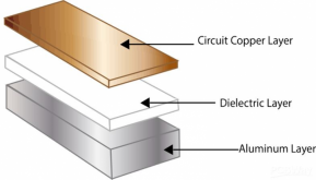
For the fets I am planning to have a daughter board only for the fets. I would like to try aluminum core PCB. I will use smd fets.
1611078044289.png
The dielectric layers is thermally conductive and electrically isolant. Mosftes will be mounted on the top, copper side. This kind of PCB is usually used in high power diodes for proper dissipation.

Maybe this is not the easiest solution but this is a hobby project and I want to try it. You can think they are expensive but they are not. I need to double check the prices anyway. If it is more than I think I will go for normal FR4 with 2-3oz copper.
Active balancing:
For large packs that need a larger amount of balancing in perpetuity it is worth active balancing, mostly so as a designer you dont have to deal with as much heat dissipation on the pcb, but the efficiency and speed advantage is a bonus.
Chips like the ETA3000 work well, but there is a fundamental flaw when using them in large packs. Because each chip only senses its cell and the one higher, and balances to 30mv, you can end up where they are no longer transferring current in this scenario: 4.11 4.13 4.15 4.17 4.19 4.21 4.23. Each chip thinks it is balanced to 20mv, but the pack is well out of balance.
The chips internally are just synchronous buck converters with the feedback point of (vc1+vc2)/2 with a bit of hysteresis and current limiting.
What really needs to happen is that the main MCU synchronizes all of them and tells them what direction to run to balance the whole pack, and to make use of the high accuracy ADC in the BQ chip to shuttle charge to end up with an accurate final balance. This could also run when the pack isn't just at balance voltage.
I am still not sure if active balancing is useful. Talking about the voltage curve, in the knees is useful for sure but in the central region where the curve is flat.

Videos where people test balancers always test them with the pack disconected. This means internal resistance does not have effect in the voltage accross the cell. If resistance of the cells is perfectly matched, this will work also perfectly during charging and discharging because internal resistance will create the same voltage drop under current in every cell. If resistances are not perfectly matched, they will produce different voltage drops, resulting in different cell voltages even they the have the same state of charge. This will trigger the balancer during charge and discharge unbalancing the cells. There are many studies about this. I have seen many people saying that they are using them and their voltages are the same for every cell but I doubt the cells are SoC balanced.

Maybe I am totally wrong but if I want to do something, it needs to be something different to what there is in the market. Talking about a balancer, where you have converters and currents that need to be controller I am not going to put effort untill I am sure that it is really needed.

I was thingking that a solution for this could be do periodical top balancing with the active balancer. Once every 1 or 2 months battery pack is charged over the knee and the balancer would do the top balancing.

ETA3000 neughbour balancing. Only balances with the neighbour cell. If the top needs top balance with the bottom, all of them need to work moving current cell to cell from top to bottom. It is exactly the one Will used in his video

They do not really need MCU, they work autonomous.

My idea for active balancing is also using buck converters but in a different way. It works in simulation (matlab simulink with real battery models). But I am not planning to implement it for now.

Software:
For the Coms, bluetooth is only useful if there's a companion app that can be used to see and set parameters for mobile/portable applications
Wifi would be great, would be useful to be able to transmit Voltages, currents, SOC, Balance accumulation, ETC over mqtt. This can permit logging with Emoncms, or grafana/influx. Or integration in to other systems.
A specified UART protocol could be useful.
Most flexible would be making the main mcu arduino compatible, opens up tweaking the code to customise the operation to a wider audience.
Id likely try use an ESP32 for the Main mcu, which can easily do bluetooth & wifi if needed, and should be more than fast enough to interface with the BQ chip.
It would also be needed to have some way to edit the calibration values for cell voltage measurements.

I think I will go with ESP32. I am not a big fan of it. This can also replace the STM32 main MCU. In terms of of open source is convinent as it can be programed with Arduino IDE. I would not like to use it but I think it is the most convinent solution. It will also reduce the BOM.

I see little need for the SOC Mcu or the balance mcu, the Main mcu should have no problem reading that info from the BQ and passing it to where is needed. The added complexity of all the communication between the different MCUs would be unlikely to outweigh the benifits of a dedicated mcu for the task.

I am not worried about that. Comunications with DMA are very efficient.

Keen to help out where needed on this design, it really would benefit being open source and means that wherever the design gets to it can be taken over by someone else.
Thank you for your help. I do not mind making it opensource.
 
Last edited:
You're using a really cheap battery monitor chip. Is that the best choice? You'll be putting a lot of effort into this design. You don't want to be limited due to an "average" or "sub-average" monitor chip. The listed data sheet application choices don't sound too overwhelming. Looking at the voltage reference, it specs +/- 10 LSB error over temperature. Is that acceptable? I'm designing a BMS, using a ADS1115 16 bit adc. I'm not happy with the thermal drift performance. I'll probably switch to another adc that has an external voltage ref.
 
This concept seems reasonable, but nothing stands out as an advantage over systems already out there. While Batrium is fairly expensive compared to the low-end Chinese products - it is cheap compared to designing your own from the ground up.

When I was kicking around my own ideas to design a BMS, my only motivation was based on the likelihood that I could make something genuinely better for my application. By the time I worked out a block diagram, I realized that doing it for 'economics' was cognitive dissonance at work. I was hoping to improve existing designs in both accuracy (primarily for accurate coulomb counting), and extremely robust design among other goals. Of course lofty goals create lofty engineering issues that have to be solved. Looked like too much work for a hobby project and I don't want to start a BMS business either.

Perhaps just for fun, challenge, learning?
 
My favorite thing about the ESP32 is that it has good MicroPython support that allows you to get a fairly complex application up and running REALLY fast compared to C/C++ that still dominates in the embedded world. For the management tasks needed in this application, you will not run into performance issues. All the hard stuff is done by dedicated silicon that just hands off the final results.
 
You're using a really cheap battery monitor chip. Is that the best choice? You'll be putting a lot of effort into this design. You don't want to be limited due to an "average" or "sub-average" monitor chip. The listed data sheet application choices don't sound too overwhelming. Looking at the voltage reference, it specs +/- 10 LSB error over temperature. Is that acceptable? I'm designing a BMS, using a ADS1115 16 bit adc. I'm not happy with the thermal drift performance. I'll probably switch to another adc that has an external voltage ref.
Cheap does not mean bad. Do not think that 1k$ use better chips. Price of chips is mainly driven by mass production, not only by quality.
 
Last edited:
This concept seems reasonable, but nothing stands out as an advantage over systems already out there. While Batrium is fairly expensive compared to the low-end Chinese products - it is cheap compared to designing your own from the ground up.

When I was kicking around my own ideas to design a BMS, my only motivation was based on the likelihood that I could make something genuinely better for my application. By the time I worked out a block diagram, I realized that doing it for 'economics' was cognitive dissonance at work. I was hoping to improve existing designs in both accuracy (primarily for accurate coulomb counting), and extremely robust design among other goals. Of course lofty goals create lofty engineering issues that have to be solved. Looked like too much work for a hobby project and I don't want to start a BMS business either.

Perhaps just for fun, challenge, learning?
Price of devices are mainly derived from engineering costs, not BOM. The BOM I am proposing will be lower than 100$.
I do not do it for challenge or learning as it is a very basic project for an electronic engineer. It is just putting many componets together on a PCB in a field that it is deeply explored.
I do it for fun.
 
Last edited:
You're using a really cheap battery monitor chip. Is that the best choice? You'll be putting a lot of effort into this design. You don't want to be limited due to an "average" or "sub-average" monitor chip. The listed data sheet application choices don't sound too overwhelming. Looking at the voltage reference, it specs +/- 10 LSB error over temperature. Is that acceptable? I'm designing a BMS, using a ADS1115 16 bit adc. I'm not happy with the thermal drift performance. I'll probably switch to another adc that has an external voltage ref.
16 bit adc I think is an overkill. Using the ingernal PGA you can have an input range of 512mV divided by 2^16 means that you can get a resolution of 8uV. Of course those are the bits not the ENOB (effective number of bits) so resolution will be degradated. I think for this kind of applications you do not need that resolution.

For me 1mV could be good but 10mV for this application I think it is enough.

External reference is always the best but depends on the application.
 
The BQ76952 coulomb counter is setup for a 200mV range - which is rather big for a high-current system.

If you take advantage of the full range (which is definitely needed with the integrated ADC), 200A would be creating a 40W problem with your sense resistor. Ouch. A 400A system would really get scorching hot.....
 
Price of devices are mainly derived from engineering costs, not BOM. The BOM I am proposing will be lower than 100$.
I do not do it for challenge or learning as it is a very basic project for an electronic engineer. It is just putting many componets together on a PCB in a field that it is deeply explored.
I do it for fun.
Just talking about this, I could show you a victron MPPT and you can see that the BOM of the PCB is quite quite cheap. It uses very standard components but what you pay is the time of the engineers.
 
16 bit adc I think is an overkill. Using the ingernal PGA you can have an input range of 512mV divided by 2^16 means that you can get a resolution of 8uV. Of course those are the bits not the ENOB (effective number of bits) so resolution will be degradated. I think for this kind of applications you do not need that resolution.

For me 1mV could be good but 10mV for this application I think it is enough.

External reference is always the best but depends on the application.
16bits (even roughly implemented with weak ENOB) is fine for monitoring and balancing. The accuracy is needed on the coulomb counting side of the circuit - which requires rather high accuracy to be functionally useful in the real world.
 
The BQ76952 coulomb counter is setup for a 200mV range - which is rather big for a high-current system.

If you take advantage of the full range (which is definitely needed with the integrated ADC), 200A would be creating a 40W problem with your sense resistor. Ouch. A 400A system would really get scorching hot.....
You are right but that does not mean you need to use tho whole range. In any case as I already said this is only an initial draft, I need to sit down, check every options in the market and decide which one is the best.
 
16bits (even roughly implemented with weak ENOB) is fine for monitoring and balancing. The accuracy is needed on the coulomb counting side of the circuit - which requires rather high accuracy to be functionally useful in the real world.
Of course, I can always split BQ76952 in different dedicated components and get better performance.
 
Just talking about this, I could show you a victron MPPT and you can see that the BOM of the PCB is quite quite cheap. It uses very standard components but what you pay is the time of the engineers.
True - but you have already claimed this is simple stuff and the software will only take a day.

Just to put it out there, I am also an engineer. A mixed discipline engineer that splits ME and EE (and soon CS). About 50% of my EE work has been in high-reliabilty power electronics. None of it is quick or simple even when it seems quick and simple on the surface.

I worked with an engineer that tended to over-simplify everything and supported his simplifications with crude prototypes that could demonstrate something on a bench. When it came time to make a complete system - it took a dozen people months to 'make it right'. In the hobby realm, many corners can be cut but the basics still apply.
 
You are right but that does not mean you need to use tho whole range. In any case as I already said this is only an initial draft, I need to sit down, check every options in the market and decide which one is the best.
True, but you are already starting with modest resolution for a coulomb counter. If you truncate the range, you are really just going to end up with a loose guess at coulomb count. Why bother?

I see coulomb counters as a critical element in a battery system. The shitty one on my Chargery BMS is so bad, I just ignore everything it says and added a Victron Smart Shunt which is functionally accurate.
 
As I do not want to publicly show my work I can show you it in private. For example today I have done the schematic of a testboard more complicated than this. I have also met people who overstimate the work something takes just because they do not have the expertise. It happens to me a lot for example. Everytime I need to work with chemicals I take weeks for something my colleages do in one day because they do it in daily base.
 
True, but you are already starting with modest resolution for a coulomb counter. If you truncate the range, you are really just going to end up with a loose guess at coulomb count. Why bother?

I see coulomb counters as a critical element in a battery system. The shitty one on my Chargery BMS is so bad, I just ignore everything it says and added a Victron Smart Shunt which is functionally accurate.
Have you updated to the latest firmware? ..... It was really bad, but they improved it quite a bit.
 
True, but you are already starting with modest resolution for a coulomb counter. If you truncate the range, you are really just going to end up with a loose guess at coulomb count. Why bother?

I see coulomb counters as a critical element in a battery system. The shitty one on my Chargery BMS is so bad, I just ignore everything it says and added a Victron Smart Shunt which is functionally accurate.
I do not know why I post things. I always that it can be a candidate and people take it as I am going to do it even if the world ends tomorrow.

I will repeat again, this is a DRAFT (and maybe not even that).

It can be done quick if time is dedicated, but now I am only dedicating 10 minutes per day.

The first step is to target the required features and that is why I created the post. I am still in that phase, not with the component selection phase.

I just posted a high level diagram as reference.
 
Have you updated to the latest firmware? ..... It was really bad, but they improved it quite a bit.
I have not. Honestly, I am a bit nervous about bricking the unit before I have another one ready to go.
 
Back
Top