You are using an out of date browser. It may not display this or other websites correctly.
You should upgrade or use an alternative browser.
You should upgrade or use an alternative browser.
Cal's DIY BMS
- Thread starter Cal
- Start date
Not sure for the ESP32, I'm not used to them, I recommend to check in the datasheet to be 100 % certain.
You can also try to disconnect SDO as close to the ADC as possible and scope it. If it's fine then it's something down the line who is pulling it down.
You can also try to disconnect SDO as close to the ADC as possible and scope it. If it's fine then it's something down the line who is pulling it down.
Good call! Apparently the ESP32 was holding the adc SDO signal low. I lifted the wire at adc SDO and voila, the signal appears. Channel 2 of plot is SDO at the adc. Not many advantages hand wiring the circuit. But for troubleshooting, being able to lift any signal is a major advantage.

Currently the SPI clock is operating at 100 kHz. Max clock for the adc is 2 MHz. Since adc conversion time is 17 ms, a 100 kHz clock really won't slow the process down. To send 16 bits takes 160 us at 100 kHz. @BiduleOhm, what SPI clock rate are you planning on using?
Edit: I see my error: MISO (pin 19) and MOSI pin 23) are swapped. ADC SDO output was connected to pin 23 which is MOSI. SDO needs to be connected to pin 19 (MISO).
Last edited:
Good call! Apparently the ESP32 was holding the adc SDO signal low. I lifted the wire at adc SDO and voila, the signal appears. Channel 2 of plot is SDO at the adc.
Ok, perfect
Currently the SPI clock is operating at 100 kHz. Max clock for the adc is 2 MHz. Since adc conversion time is 17 ms, a 100 kHz clock really won't slow the process down. To send 16 bits takes 160 us at 100 kHz.
Be careful, the conversion can take up to 23 ms (with 17 ms being the typical time). You can either use a 23-24 ms timer or check the status if you want to sample as fast as possible (see datasheet page 10; you must use an idle high clock, pulling CS low, SDO will be high if busy or low if finished).
@BiduleOhm, what SPI clock rate are you planning on using?
I plan to go for around 1 MHz so I waste as little time as possible doing data transfer. I'll not go for the 2 MHz max just to be safe and also because the MCU will likely not go that fast anyway (I'll have to read a pin and have a condition in the while() so it'll be slower than this example even without the NOPs).
Things are moving along.
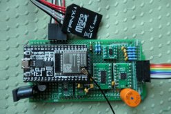
I've added a data logging function. Logging is extremely important for design validation and troubleshooting. Bottom left is 5V input power for the ESP34 and logic chips. I was able to remove the power plug from a defective Arduino Uno. Next to the plug is a 47 uF cap which is also removed from Uno. Off to the far right is an orange 45-year old 47 uF cap (to filter battery voltage) from my days working at Bosch. The ribbon cable on the right connects to the individual cells.
I'm impressed with modern day parts. For example, modern IC's have gnd and power pins are right next to each other. That makes connecting bypass caps extremely easy. In the old days, power and gnd were located at opposite ends of the IC, making bypass caps less effective.
Capacitors have also gotten a lot smaller. I got 0.1 uF, 50V yellow caps scattered the circuit. They fit nicely between two adjacent IC header pins.
So far with this setup I can measure 4 cell voltages and log data. There's no provision to measure total battery voltage yet. I need to add a resistive voltage divider and run it through the adc, or get voltage readings from the INA226. The INA226 contains a 16-bit adc that measures both shunt current and battery voltage. The INA226 still needs to be connected to the board via I2C communication. INA226 will be located near the shunt.
There is a cell measurement issue.
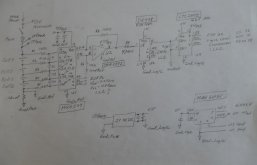
Once U1 (MUX509) control pins are selected to access specific cell voltages there's a 5 ms delay and then a adc conversion is made. At that point in time voltage measurements are way off base.
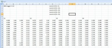
This excel plot shows 4 measurements each of cell1 through 4. Once the 16 measurements are made there's a 1 second delay and then a new line shows the same sequence over again.
The first data for V1 is 4.098V, delay of 25 ms, then 3.64V, delay 25 ms, then 3.399V, delay 25 ms then 3.313V.
Cell 2 starts with 4.072V, 3.977V, 3.54V, 3.407V.
We're seeing an exponential voltage decay.
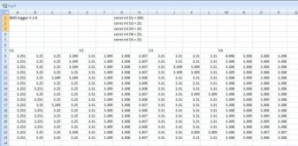
This data shows a 200 ms delay (instead of 5 ms). The 200ms delay is enough time for the voltage to decay and stabilize.
It looks to me as if the front end filter (100k ohm, 0.1 uF) is too large. Perhaps the cap needs a 10x or 100x reduction?

Once U1 (MUX509) control pins are selected to access specific cell voltages there's a 5 ms delay and then a adc conversion is made. At that point in time voltage measurements are way off base.

This excel plot shows 4 measurements each of cell1 through 4. Once the 16 measurements are made there's a 1 second delay and then a new line shows the same sequence over again.
The first data for V1 is 4.098V, delay of 25 ms, then 3.64V, delay 25 ms, then 3.399V, delay 25 ms then 3.313V.
Cell 2 starts with 4.072V, 3.977V, 3.54V, 3.407V.
We're seeing an exponential voltage decay.

This data shows a 200 ms delay (instead of 5 ms). The 200ms delay is enough time for the voltage to decay and stabilize.
It looks to me as if the front end filter (100k ohm, 0.1 uF) is too large. Perhaps the cap needs a 10x or 100x reduction?
That's weird.
The caps are always connected to the cells and they aren't switched by the MUX so they're always at the cell voltage. I would expect the behaviour you have if there was only one cap on the output of the MUX but I thought about that and that's precisely why I put them before it.
What happens if you by-pass the DG408? and what happens if you remove the cap on the ADC input?
Last edited:
Yes, next step is to remove the caps and see what happens.
Here's a scope plot of voltage at input to adc. The mux first connects cell 4 to the adc, then 3, etc. The voltages correspond with the 5 ns delay excel plot. Cell 4 has a rising exponential curve while cells 3 - 1 have a decaying exponential curve..
It sure looks like the time constant of the voltage decay corresponds to the 10 ms or perhaps 20 ms time constant of the input filter.
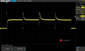
Hey, I'm glad you talked me into increasing the current limit resistor R8 to 470 ohms. U3 (DG408) is seeing an overvoltage.
Here's a scope plot of voltage at input to adc. The mux first connects cell 4 to the adc, then 3, etc. The voltages correspond with the 5 ns delay excel plot. Cell 4 has a rising exponential curve while cells 3 - 1 have a decaying exponential curve..
It sure looks like the time constant of the voltage decay corresponds to the 10 ms or perhaps 20 ms time constant of the input filter.

Hey, I'm glad you talked me into increasing the current limit resistor R8 to 470 ohms. U3 (DG408) is seeing an overvoltage.
One recomendation I could make is replacing opa991 with an instrumentation amplifier with the same gain. Now you are using the filter resistors together with R7 and R6 to create a difference amplifier. It should not be a big problem but mux is not transparent and you can introduce innacuracies in your measurements because you are taking it into the equation. Using an INA you will have high input impedance neglecting the mux innacuracies with the same result.
You can see in figure 8 of MUX509 datahseet how on-resistance is dependant with the pin input voltage. This missmatch will create an offset in the output different for every cell. It can be considered marginal compared with the 100k resistor but I just wanted to let you know.
One recomendation I could make is replacing opa991 with an instrumentation amplifier with the same gain. Now you are using the filter resistors together with R7 and R6 to create a difference amplifier. It should not be a big problem but mux is not transparent and you can introduce innacuracies in your measurements because you are taking it into the equation. Using an INA you will have high input impedance neglecting the mux innacuracies with the same result.
The MUX Ron mismatch is far below the 100k resistors tolerance so that shouldn't be a problem
Edit: ah, didn't saw your following post.
I read now that your input filter is 100k ohm, 0.1 uF and maybe the lack of high input after the mux is producing high inrush current discharging and charging the filter capacitor when the mux is switched. You will need to probe it with the oscilloscope. This is just a guess.
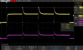
Good to see that you found the problem. I am 95% sure that replacing opa991 with an INA you will solve the problem because what I said. (maybe there is something else)Yellow trace is adc in. 2V/div
Purple trace is OpAmp out. 5V/div
I put the horizontal cursors on the yellow trace to measure peak voltage (5.8V). The protection diodes are conducting at this time.
Tomorrow I'll remove the input caps. Trace should look better then.
I read now that your input filter is 100k ohm, 0.1 uF and maybe the lack of high input after the mux is producing high inrush current discharging and charging the filter capacitor.
What is "high input"?
If you're talking about the MUX or op-amp input capacitances, they are in pF so negligable.
View attachment 42069
Yellow trace is adc in. 2V/div
Purple trace is OpAmp out. 5V/div
I put the horizontal cursors on the yellow trace to measure peak voltage (5.8V). The protection diodes are conducting at this time.
Tomorrow I'll remove the input caps. Trace should look better then.
Ok, something weird is going on.
Can you scope the op-amp inputs on the same capture (ideally with a faster timebase, something around 10 ms/div)? I wonder if there's a delay between both halves of the MUX...
Good to see that you found the problem. I am 95% sure that replacing opa991 with an INA you will solve the problem because what I said. (maybe there is something else)
I don't see how an INA would solve that problem (especially since we still don't know from where it comes exactly). As said, it's not the MUX Ron mismatch since it would be less than a fraction of a % and it wouldn't be a transient, it would be continuous.
Good to see that you found the problem. I am 95% sure that replacing opa991 with an INA you will solve the problem because what I said. (maybe there is something else)
I'm not sure I found the problem. You think the problem is the OpAmp? What makes you believe that?
How input impedance sorry.What is "high input"?
If you're talking about the MUX or op-amp input capacitances, they are in pF so negligable.
How input impedance sorry.
Input impedance of the op-amp is at worst multiple dozens of GOhms so I think that's high enough ^^
Similar threads
- Replies
- 8
- Views
- 518
- Replies
- 6
- Views
- 445
- Replies
- 40
- Views
- 2K
- Replies
- 4
- Views
- 353


