diy solar

diy solar

DIY 6 kVA 48V inverter using low freq transformer

AntronX

DC Powered
Joined
Oct 24, 2021
Messages
1,422
Location
South FL
Hi, I have big and heavy low frequency 27V > 120/240V toroidal transformer from parted out Xantrex 6048 inverter. I would like to make MOSFET H-bridge inverter and PWM controller to drive it. So far I found IPP016N08NF2S 80V 196A 1.6mOhm MOSFETs on mouser that look pretty good for low frequency commutation side at least. I may have to model their switching losses at PWM freq or look for other FETs with acceptable switching loss for high side of the H-bridge.

Has anyone here done this kind of project? Any pointers for controller software, gate driver and current protection? I would like this to be a pure sine wave inverter.

Thanks.
 
This is done all the time, and its fairly straightforward.
Suggest you do an internet search for "The Back Shed, Oz inverter". The Australians on The Back Shed Forum have built literally hundreds of these over the last few decades, and its all gradually matured into a very efficient and reliable design.

A couple of tips from an old hand...

I suggest you hook up your big transformer to the grid and measure the no load idling power. Some commercial transformers of that size can have a surprisingly high idling power, possibly well in excess of 100 VA. That transformer will work fine for you, but its probably going to chew through a lot of battery capacity at night with such a hungry greedy transformer.
The state of the art these days for a 6KVa inverter with home wound toroidal transformer would be a zero load idling power of around 25 to 35 Watts. If high idling power becomes an issue, a winding a more efficient transformer yourself, might be worth thinking about later on.

Second tip, those Mouser mosfets are nice at 1.5 milliohms, but I bet they are expensive.
I suggest you initially try some cheapy Chinese HY4008 mosfets. These are 2.9 milliohms and 80 volts, and will work fine for an initial prototype. If you blow up a few testing, its no great loss. Once all the Gremlins are finally sorted out, you can upgrade to the more expensive mosfets at a future date.
 
Last edited:
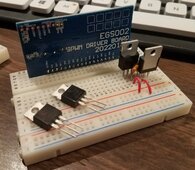
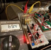
OK this project has begun. Testing EGS002 board. It works with voltage and current feedback bypassed. Getting 8.6Vac out with 12Vdc in. Feeding small 120v>12.6v transformer. Will enable and test V/I feedback next before moving on to bigger mosfets.
20240401_230610_resized_1.jpg 20240402_114059_resized_1.jpg
 
Last edited:
I suggest you hook up your big transformer to the grid and measure the no load idling power. Some commercial transformers of that size can have a surprisingly high idling power, possibly well in excess of 100 VA. That transformer will work fine for you, but its probably going to chew through a lot of battery capacity at night with such a hungry greedy transformer.

Backfed VA may differ from forward fed. It certainly does for the utility transformers I've tested. If you have a buck-boost transformer, that could put out 24Vrms to test the other direction. Variac even better, crank up and study current draw.

If you have a fancy enough scope, graph integral(V) vs. current, that is the BH curve. Or capture waveforms and post process. You can take parameters off the graph for a Chan SPICE model. Difficult enough for me the first time around I relied on measurements to characterize chokes. Later managed to make models that reasonably predicted behavior.

I would like to make MOSFET H-bridge inverter and PWM controller to drive it.

Are PSW inverters implemented as PWM into a transformer? Or PWM into an inductor, making a buck converter to apply sine wave to the transformer?

I've only implemented low powered amplifiers, but I used diodes to protect transistors from flyback beyond the rails. A previous model reportedly blew out the transistors anytime someone unplugged it under load. (instrument/sensor application.)
 
Are PSW inverters implemented as PWM into a transformer? Or PWM into an inductor, making a buck converter to apply sine wave to the transformer?
PWM into filter inductor in series with transformer primary. Same way it's done with all LF transformer inverters. Using this simple circuit from EG8010 datasheet for now. Will include filter inductor once i get to high power build. There are threads on here about filter inductor design for diy inverters I will have to find again.
EG8010_LF.PNG
 
Backfed VA may differ from forward fed. It certainly does for the utility transformers I've tested. If you have a buck-boost transformer, that could put out 24Vrms to test the other direction. Variac even better, crank up and study current draw.
Yes, leakage inductance plays a part.
But we do not need super accuracy here.
Just to know if some unknown "lump" is going to be a likely candidate for an inverter, or totally useless.
 
Yea I don't like their current limit implementation. I will test it at safe levels to see how it performs but I'd like to redesign it.
The EGS board is a very good way to get started, but there are some known shortcomings....
As you have noted the current limit is a bit sus.
The other problem is, if you blow a power mosfet, that will kill the gate driver chip on the EGS board every time, and likely put full dc battery voltage onto the +12v supply.
That can be most unfortunate !

A solution that definitely works is to use the gate driver chip on the EGS board to drive the LEDs in some opto isolated gate driver chips.
The opto isolators then sacrifice their lives to save all the low voltage control circuitry in the event of a blow up.

Place the opto isolators close to the mosfets, and run a twisted pair to the LEDs. That will hugely reduce noise problems in the gate drive, especially if your large heatsinks are running "live" and not grounded.

Its usually possible to get away with noise and quite a few other problems in a low powered prototype.
Once you get past that stage, it all becomes a lot more serious (and difficult) at much higher power levels.
 
A solution that definitely works is to use the gate driver chip on the EGS board to drive the LEDs in some opto isolated gate driver chips.
Good idea. I also don't like stock drivers only having 2A drive current rating. That's not enough to drive large mosfets to their rated switching speed or multiple in parallel. For large banks of mosfets I will have to implement a discrete push/pull buffer stage.
 
Good idea. I also don't like stock drivers only having 2A drive current rating. That's not enough to drive large mosfets to their rated switching speed or multiple in parallel. For large banks of mosfets I will have to implement a discrete push/pull buffer stage.
Don't go crazy with the switching speed. TO-220 case has quite a bit of lead inductance and it SUCKS with high current if you attempt to push the switching speed anywhere near "rated" in transistor datasheets. There is a bit of risk also "banging" the opposite mosfet body diode too hard and cause excessive losses or device failure because of reverse recovery.

Your proposed mosfet looks decent enough albeit I'd select one with more voltage margin.
Stay away from the latest ultra low rds-on mosfets, those seem to have worse reverse recovery and avalanche ratings. (Infineon Optimos series vs. StrongIRFET series)

BTW: Diyaudio.com forums have couple of excellent class-D amplifier threads somewhere under all that nonsense that cover the power stage device selection really well. (Inverter H-bridge is pretty much same as class-D amplifier, just more crude and typically with more power)

Not a fan of the IR2110 drivers, those are bit picky and prone to destruction with ground bounce. Back-to-back connected optocouplers or "simulated" optocouplers give foolproof interlocking that prevents shoot-trough. Plenty of options, this one for example looks interesting https://www.digikey.fi/fi/products/detail/texas-instruments/UCC23313DWYR/10715550
Crazy good common-mode transient immunity, decent output current capacity
 
TO-220 case has quite a bit of lead inductance and it SUCKS with high current if you attempt to push the switching speed anywhere near "rated" in transistor datasheets.
Thanks for your info! What do you think of paralleling a bunch of these mosfets? They seem cheapest option per Amp (ignoring Chinese TO-247): Toshiba TPH3R70APL 100V 150A, Mouser $1.31/pc. GS Vth is only 2.5V whould that be an issue at parasitic triggering?
 
Not a fan of the IR2110 drivers, those are bit picky and prone to destruction with ground bounce. Back-to-back connected optocouplers or "simulated" optocouplers give foolproof interlocking that prevents shoot-through. Plenty of options, this one for example looks interesting https://www.digikey.fi/fi/products/detail/texas-instruments/UCC23313DWYR/10715550
Crazy good common-mode transient immunity, decent output current capacity
Have to agree, the IR2110's are a bit of a worry.
What happens, if the mosfet blows, often putting full battery voltage onto the mosfet gate.
The IR2110 also blows, then putting full battery voltage onto the +12v supply.
The carnage then rapidly spreads further......

Back to back inverse connected opto isolated gate drivers offer several advantages. With a suitable capacitor, it will very simply generate symmetrical dead time, and offer absolutely fool proof shoot through protection. Opto coupled gate drivers also prevent any blow up from propagating back into the low voltage driver part of the circuit as well as providing very high noise immunity.

The original inverse opto circuit (first used in my Warpverter design) is now been adopted by many other inverter designers/builders with great success, as its becoming more widely known about.
 
Last edited:
Thanks for your info! What do you think of paralleling a bunch of these mosfets? They seem cheapest option per Amp (ignoring Chinese TO-247): Toshiba TPH3R70APL 100V 150A, Mouser $1.31/pc. GS Vth is only 2.5V whould that be an issue at parasitic triggering?
Seem like pretty low gate charge, should be easy to drive. But not great fan of logic-level gates with high power switch-mode power supplies.
max rated avalanche energy lot lower than your original proposal, body diode reverse recovery characteristics look also less than stellar

SMD case like that you need to get creative with cooling. with 1 or 2 devices and 5w of power losses you can dissipate the heat in the pcb copper pours, 6kW inverter with 50....200W total losses in mosfets not so much.
 
max rated avalanche energy lot lower than your original proposal, body diode reverse recovery characteristics look also less than stellar
Thanks. Any good cheap transistors you can recommend? I don't want to buy Chinese brands because the only way to get them is via Ebay or Ali and I am concerned I will buy fakes. Also looking at data sheet for HY4008 it looks too good to be true in some parameters compared to name brand devices. I found FDP053N08B 80V 120A 5.3mOhm TO-220 for $1.68 ea. 65nC gate charge, 4480pF gate cap, 2.5 - 4.5V Vgs(th), 60ns 63nC diode reverse recovery, 1.3V max diode forward voltage at 75A, 365mJ avalanche. Which other parameters should I be looking at for inverter H bridge application?
 
Last edited:
Maybe there is a TO-247 version of that available ?
Exact same die, but should have a lower thermal resistance and fatter legs.
A slightly higher cost but adding more robustness ?
 
Maybe there is a TO-247 version of that available ?
None that I could find without breaking the bank. TO-247 packaged transistors are way more expensive. This one is package limited to 75A continuous which is not bad since I will parallel them anyway. 1°C/watt thermal resistance is not great but I don't expect more than 20 watts of dissipation per device.
 
This seem to be good example how everything else than Qgd*Rdson goes to worse when moving from Optimos 3 generation to Optimos 5

As to what I would suggest IRFB4410 is tried and tested model with better body diode specifications than most
Note that this has reverse recovery specified at 125C temperature unlike most others!


5 parallei would keep the H-bridge conduction losses at 100A around 40W.
 
Back
Top