diy solar

diy solar

DIY All-In-One Solar Generator - Control Board

Also we're talking about an on-board ADC with only 12 bits and an internal Vref (which is notoriously crappy...)

I used an external 1 ppm Maxim voltage reference, also oven-controlling it to within a couple of degrees.
Guess how stable a 1 ppm reference is?
... about 4 ppm/degree, at some temperatures. Turns out that one I selected was 1 ppm at room temperature. I heated it to about 85C where it was 2 ppm, but controlled with 2 degrees I probably got 4 ppm out of it.

That famous 0.05 ppm voltage reference from LTC that's used in the highly stable meters is actually a 1 ppm reference, with heater and temperature sensor for a roll-your-own oven-stabilization circuit. Convenient because its thru-hole package provides thermal isolation. For my SMT design I put thermal reliefs in the PCB planes and layered insulation top and bottom. Took about 3 watts to overcome the heat loss it still had, over a moderate ambient environment. But it got my RF circuit stable to 100 ppm of amplitude. It was more than just the voltage reference which required oven stabilization.

Crystals, it turns out, when spec'd as stable to 3 ppm aren't 3 ppm/degree, they're 3 ppm over entire operating temperature range. That is achieved with positive/negative balancing for temperature compensated TCXO. Doesn't even need oven stabilized OCXO.
 
The impedance I propose to him was actually 2M || 100k || 100k = 48.78k (thevenin equivalent impedance) which should be fine for driving a high-impedance analog input. At least in terms of DC. Some unbuffered ADC inputs charge a sampling cap, so capacitor across the input supplies that in addition to being part of an RC filter.

I checked the datasheet and the leakage current is 1 µA max so it would be 2 V across a 2 M resistor (I know, I know, it's not exactly that, I just want to do a rough estimate). So if the PV voltage is 40 V that would mean a 5 % error.

Good point on oversampling. There's a lot more bits available so long as you have enough random noise. Maybe don't decouple inputs as well as I suggested? I've put capacitors on ADC inputs, and I've oversampled data into a scope, but I haven't played with input capacitance vs. recovering more bits resolution than is native to the ADC.

Yep, it's a rare instance where we want noise (but only random one...), IIRC anything above 2 LSB (2.44 mV here) is good enough.
 
I used an external 1 ppm Maxim voltage reference, also oven-controlling it to within a couple of degrees.
Guess how stable a 1 ppm reference is?
... about 4 ppm/degree, at some temperatures. Turns out that one I selected was 1 ppm at room temperature. I heated it to about 85C where it was 2 ppm, but controlled with 2 degrees I probably got 4 ppm out of it.


Interesting, 85 °C is pretty high for a reference oven. Well, as long as you had the accuracy you wanted it's fine ;)

That famous 0.05 ppm voltage reference from LTC that's used in the highly stable meters is actually a 1 ppm reference, with heater and temperature sensor for a roll-your-own oven-stabilization circuit. Convenient because its thru-hole package provides thermal isolation. For my SMT design I put thermal reliefs in the PCB planes and layered insulation top and bottom. Took about 3 watts to overcome the heat loss it still had, over a moderate ambient environment. But it got my RF circuit stable to 100 ppm of amplitude. It was more than just the voltage reference which required oven stabilization.

Yep, they're also aged and sorted before being put in the test equipment, that's part of the sky high price...

Crystals, it turns out, when spec'd as stable to 3 ppm aren't 3 ppm/degree, they're 3 ppm over entire operating temperature range. That is achieved with positive/negative balancing for temperature compensated TCXO. Doesn't even need oven stabilized OCXO.

Yeah, you need to be really careful when reading those kind of specs in a datasheet, a mistake happens quickly.
 
Interesting, 85 °C is pretty high for a reference oven. Well, as long as you had the accuracy you wanted it's fine ;)

I think it was more like 60C oven up to 45 degrees "ambient" measured elsewhere on the PCB, then a range switch to 80C if the board ran hotter. I didn't quite achieve the temperature rise necessary to pick a single operating temperature over a wide environment. FR4 and skinny copper traces are a better conductor of heat than you would expect. Would be better on a daughtercard.

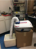
For a mass spec. I was initially asked to achieve 0.1% accuracy on DC grid voltages and RF amplitude. Also filament emission of 0.1%. Turned out 0.1% emission stability required 1 ppm voltage control (over thermal time constants.) Achieving 0.1% accuracy of ion currents through quadrupole filter (gas composition in something like a smog-check machine) required 100x better stability, about 10 ppm, for the electrical signals. So I had to sharpen my pencil and play a few more tricks. Like those Vishay resistors, and others to zero out drift of DAC and op-amps. Told the boss he'd have to rent the $10,000 8.5 digit HP/Keysight DMM to measure what he wanted me to achieve, and keep doors closed to stabilize room within 2 degrees while I cycled my DUT over a +/- 20 degree spread. Wasn't even given an environmental chamber, so I built my own out of a turkey roaster and ice bucket.

I didn't quite achieve the 0.5 ppm/degree regulation of DC voltages I was trying for (+/-10 ppm over +/- 20 degrees C), but I did demonstrate 1.0 ppm/degree.

1597774948441.png

“Although a reference with temperature drift of 0.05 ppm/°C is nothing short of fantasy …”
Quoted from “The 20-Bit DAC Is the Easiest Part of a 1-ppm-Accurate Precision Voltage Source”
http://www.analog.com/en/analog-dia...ac-and-accurate-precision-voltage-source.html

“building a 1-ppm system is not a task that should be taken lightly or rushed into”
Quoted from “Designing 1-ppm DAC Accuracy into Instrumentation Applications (Part 2 of 2)”
Fools rush in ...

See also: “Designing 1-ppm DAC Accuracy into Instrumentation Applications (Part 1 of 2)”
 
I think it was more like 60C oven up to 45 degrees "ambient" measured elsewhere on the PCB, then a range switch to 80C if the board ran hotter. I didn't quite achieve the temperature rise necessary to pick a single operating temperature over a wide environment. FR4 and skinny copper traces are a better conductor of heat than you would expect. Would be better on a daughtercard.

Ah ok, makes sense ;)

Wasn't even given an environmental chamber, so I built my own out of a turkey roaster and ice bucket.

:ROFLMAO: I love when the boss set high goals but doesn't want to spend a dollar...

I didn't quite achieve the 0.5 ppm/degree regulation of DC voltages I was trying for (+/-10 ppm over +/- 20 degrees C), but I did demonstrate 1.0 ppm/degree.

Very nice ?
 
It's delight to hear engineering stories and revelations behind pursuits of precision.
Although its pretty obvious but never realized what it takes to put accuracy and precision into electronic components.
A Big thumbs up (y) just for the passion.


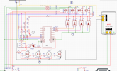
By the way I rearranged schematic as per given conventions.
Lets see if it made any difference to ease of read:

1597975456525.png

Block I denotes Battery cell electrode inputs.
Block N is the Mosfet group switching PV negative from SCC.
Block D is the Opto Driver group for balance Mosfets.
Block B is the group of Balance Mosfets themselves.
 

Attachments

  • Schematic.pdf
    188.3 KB · Views: 7
Last edited:
That's better, still very cramped in some places but better ;)

You forgot a resistor for the divider of the first cell so P1 on A7 (you also have a P1 on the cells side, that's 2 different nets, you can't have the same name for both) is directly connected to ground. But actually as it's the first cell you don't even need a divider so you can connect it directly to the MCU. It's a good idea to keep a series resistor to limit the current in case something goes wrong so keep R7, just don't connect it to ground ;)

M1-4 have their drain and source reversed because the negative side of the cells are on top on the schematic (see, that's why we put lowest potentials at the bottom; all schematic software use this orientation by default and components follow the same orientation).

You can't have only one gate series resistor (R15) as else you create a voltage divider with R17/19/20/22. You need one per mosfet between the pull-down resistor and the gate (not between the pull-down resistor and the opto).

The Vgs on M1 is marginal as its Vgsth is 2.5 V max and the opto will have a 0.6-0.7 Vce so if the cell 4 is under 3.1-3.2 V you may not turn on M1 fully. I'd recommend to use a mosfet optocoupler instead of a BJT one so you don't have the PN junction 0.6 V drop.

Not really a problem but the resistors values for the dividers to measure the cells voltages are a bit weird: we usually try to limit the number of different values components we need because it reduces assembly time and errors, and cost less as you can buy bigger quantities of fewers components values; this method is called BoM re-use. So R8/R9 can be both the same value (lets say 4.7 k as R7 is 4.7 k too) giving you a 2:1 ratio for the second cell. R11 can be 4.7 k too and R10 10 k giving you roughly 3:1 for the third cell (if you want you can have exactly 3:1 if you use two 4.7 k in series for R10 but that's a bit useless as you'll need to calibrate the values in software anyway). And for R13 4.7 k again and 15 k for R12 (or three 4.7 k in series) to have roughly 4:1 ;)
 
Last edited:
  • Like
Reactions: Cal
2) More importantly, can't find good enough P-channel FETs that could cover Vds voltage of 45-50v with safe margins
and delivery enough current without exceeding power loss limits.
From whats available - would have to put at least 10 mosfets in parallel if not more to get 30Amp continuous.
Here is the list for your ref: https://www.electronicscomp.com/index.php?route=product/search&search=p-channel mosfet

I'm curious what Vds breakdown voltage derating do you feel is a safe margin? It's been a while but I believe we've (military standard) always used 20V above max voltage. In other words, if max voltage is 50V, then fet should be rated for 70V (or greater).

What combined Rds_on resistance do you want to achieve for your switch?

I believe it's already been mentioned, do you require 2 12V zeners in parallel with the 47uF cap? Gate drive current comes from the cap.

Edit:
Solar output is listed as 45V. What is that? Voc or Vmp?
 
Last edited:
Yeah but he gets his components from a weird website were they have only a few dozens of mosfets instead of thousands, so I doubt there's the IXT one.

BTW I didn't say anything before but this website has a lot of red flags and might sell counterfeit parts. I would never buy components outside of the reputable vendors (Mouser, Farnell, Digikey, ...), especially power mosfets who are more counterfeited than other components.

I believe he said the double zeners is for redundancy. Not really useful as pretty much all the others things on the board are SPoF, but that can't hurt and zeners are super cheap anyway, so not a big deal ;)

Edit: website link: https://www.electronicscomp.com/
 
  • Like
Reactions: Cal
Ahh, got caught up with a few things;).

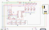
1598186454966.png

M1-4 have their drain and source reversed because the negative side of the cells are on top on the schematic (see, that's why we put lowest potentials at the bottom; all schematic software use this orientation by default and components follow the same orientation).
:ROFLMAO: Absolutely, there's surely some "rush-up" work that I despise. Thanks for the fine eye!

You forgot a resistor for the divider of the first cell so P1 on A7 (you also have a P1 on the cells side, that's 2 different nets, you can't have the same name for both) is directly connected to ground.
P1 is the same connection originating from first positive electrode on the battery going all the way to Balance Mosfet M4.
Since resource is the same - may be keeping it singleton would help reference them uniquely.

You can't have only one gate series resistor (R15) as else you create a voltage divider with R17/19/20/22. You need one per mosfet between the pull-down resistor and the gate (not between the pull-down resistor and the opto).
Well this could then be an inherent issue with mosfets in parallel configuration in general, as preceding mosfets could always interfere with voltage available to the last in series components. Have made some changes but still can't see through how best could this be done?

The Vgs on M1 is marginal as its Vgsth is 2.5 V max and the opto will have a 0.6-0.7 Vce so if the cell 4 is under 3.1-3.2 V you may not turn on M1 fully. I'd recommend to use a mosfet optocoupler instead of a BJT one so you don't have the PN junction 0.6 V drop.
M1(s) are STP90NF03L with Vgs of +/-20V driven from +12v supply from the battery itself. Vgs of +12V stemming from common ground should be high enough to activate Mosfet channel fully I believe. Do you still see it with doubt?

I'm curious what Vds breakdown voltage derating do you feel is a safe margin? It's been a while but I believe we've (military standard) always used 20V above max voltage. In other words, if max voltage is 50V, then fet should be rated for 70V (or greater).
Thats what I had in mind, with Voc of 45V anything below 70V isn't a buffer enough. May be a margin of 30% is good to restrain momentary spikes/flashes. Earlier had put a BIG 10,000 uF cap on the input supply from PVs to dampen such irregulations, but it got removed in later revisions.
What do you think - would it be good to have it?

What combined Rds_on resistance do you want to achieve for your switch?
Single digit milli Ohm scale should be fine. Anything above that isn't really meant to be used for heavy current conduction as it heats up the mosfet exponentially with linear increase in current - thus limiting the load capacity.


I believe it's already been mentioned, do you require 2 12V zeners in parallel with the 47uF cap? Gate drive current comes from the cap.

Edit:
Solar output is listed as 45V. What is that? Voc or Vmp?
Zeners in parallel are meant for redundancy.
Since they would be working much above their breakdown voltage (12v) may be putting a few in parallel could help save from unwanted surprises in field. As @BiduleOhm said - most of the design isn't contingency proof but having them wouldn't hurt either.
I am concerned about long term reliability of these zeners - probably would have to put a buck converter circuitry in place at a later stage - for now - its the zeners at duty.

45V is Voc for 24V PV panels, Vmp should be around 40V once they are fully connected to the system.

" From whats available - would have to put at least 10 mosfets in parallel if not more to get 30Amp continuous. "

That's just not correct.
You're using IRF1407: 75V, 7.8 mOhm, 130A

Here's a P-channel:
IXTH120P065T: 65V, 10 mOhm, 120A
https://www.mouser.com/Semiconducto...=1z0xv21&Keyword=20A+p-channel+mosfet&FS=True

Virtually the same specs. Just use 4 of them for a high-side switch.
Right - as already shared by @BiduleOhm, I'm working with small online stores with limited options in their inventory.
But thanks for the recommendation, if ever needed could check these ones :).

BTW I didn't say anything before but this website has a lot of red flags and might sell counterfeit parts. I would never buy components outside of the reputable vendors (Mouser, Farnell, Digikey, ...), especially power mosfets who are more counterfeited than other components.
Absolutely would agree to that, no contentions whatsoever (y) .
In the past Mosfets from some of the walk-in stores turned out to be counterfeit.
With current lockdown situation and limited mobility I'm trying multiple online local stores for components.
Some turned out to be good others no so and this one still remains to be checked.
Delivery is expected next week so would get to know their inventory.

International reputable ones are surely worth putting money on for bigger projects.
For small ones with counted component quantities their excessive shipping costs are prohibitive.
Lets see, if not would work through them as last resort.
 

Attachments

  • Schematic.pdf
    102.2 KB · Views: 7
Last edited:
P1 is the same connection originating from first positive electrode on the battery going all the way to Balance Mosfet M4.
Since resource is the same - may be keeping it singleton would help reference them uniquely.

Nope, they go through a resistor (even a voltage divider actually) so the net isn't the same. You can call them Px_DIV for example, that way you know it's Px but after being divided by some ratio.

Well this could then be an inherent issue with mosfets in parallel configuration in general, as preceding mosfets could always interfere with voltage available to the last in series components. Have made some changes but still can't see through how best could this be done?

Still not correct. R22 needs to be removed and R31-34 must be on the gate side of the junction as to not create dividers with the 10 k pull down resistors (see how you did R2-5 on F1-4 in relation to R1, you need the same topology here).

M1(s) are STP90NF03L with Vgs of +-20V and we are driving it with +12v from battery itself. With common reference voltage of +12V Mosfet channel should activate fully I believe. Do you still see it doubtful?

Nope, only the first one will receive 12 V; the second one will have 9 V, third one 6 V and the top one will have 3 V only (assuming all cells are at 3 V). Draw just the cells and the mosfets and then calculate the Vgs for each mosfet, you should see things a bit clearer ;)

@BiduleOhm said - most of the design isn't contingency proof but Still it wouldn't hurt either - but I am concerned about reliability of these zeners - probably would have to put a buck converter circuitry in place at a later stage - for now - its the zeners at duty.

Why the zeners only? I mean there's lots of other things than can fail here. Also I can't remember when I saw a zener fail, they are very very reliable. But as I said, they are cheap and don't take lots of room so if you want to put 2, no problem ;)

International reputable ones are surely worth putting money on for bigger projects.
For small ones with counted component quantities their excessive shipping costs are prohibitive.
Lets see, if not would work through them as last resort.

Farnell is free shipping once the order is past 30 € (for the .fr website, didn't look at US one) and 30 € is easy attained, even on small projects. It's thesame for Digikey but the limit is at 50 €.
 
Thats what I had in mind, with Voc of 45V anything below 70V isn't a buffer enough. May be a margin of 30% is good to restrain momentary spikes/flashes. Earlier had put a BIG 10,000 uF cap on the input supply from PVs to dampen such irregulations, but it got removed in later revisions.
What do you think - would it be good to have it?


Zeners in parallel are meant for redundancy.
Since they would be working much above their breakdown voltage (12v) may be putting a few in parallel could help save from unwanted surprises in field. As @BiduleOhm said - most of the design isn't contingency proof but having them wouldn't hurt either.
I am concerned about long term reliability of these zeners - probably would have to put a buck converter circuitry in place at a later stage - for now - its the zeners at duty.

45V is Voc for 24V PV panels, Vmp should be around 40V once they are fully connected to the system.

Been away from electronics for a while, but believe a 20V buffer above breakdown voltage is an industry standard. If Voc is 45V then 65V fets are OK to use. If you want to have added protection then a TVS diode can clamp voltage.
TVS diode

24V panels usually have Vmp = 34V. How do you figure 40V? Where's the panel spec?

How did you calculate the zener bias resistor R7?
34V - 12V / 47k ohm = 0.47 mA
Each zener is biased with 0.47 mA/2 = 0.23 mA
Is that enough current for the diode to zener?

2 zeners for redundancy? What if a diode shorts? With two installed, you got double the chance of a short.

The time constant of R7, C1 is 2.2 seconds.
Looks like the fets will slowly get adequate gate bias voltage. If you turn on the fets too early they can burn up. Doesn't appear to be a sold design.

Still like a high side switch better. No messing with panel voltage. The entire system has a solid ground. Much easier to troubleshoot.
 
24V panels usually have Vmp = 34V. How do you figure 40V? Where's the panel spec?

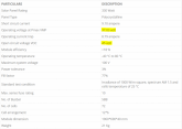
Here's the Spec sheet:
1598244611720.png

How did you calculate the zener bias resistor R7?
34V - 12V / 47k ohm = 0.47 mA
Each zener is biased with 0.47 mA/2 = 0.23 mA
Is that enough current for the diode to zener?

2 zeners for redundancy? What if a diode shorts? With two installed, you got double the chance of a short.

That R7 with 47K was there just to supply replenish/leakage current of ~1mA(45-12V) to Capacitor C1-> Mosfets.
My understanding is that Zeners work on Voltages and not on current.
Once the substrate collapses with zener voltage put across, impurities should release all free charge they have in an avalanche pattern
- making way for current flow irrespective of quantity only limited with load capacity on the higher side before burning out.
But if there is anything like Nyquist Zener current then please enlighten us and suggest how to go about it.

2 zeners for redundancy? What if a diode shorts? With two installed, you got double the chance of a short.
Well If the Zener shorts, the other one in parallel starts to conduct @12V saving system from catastrophic over-voltage failure.
So shouldn't this cut risk by half instead?

The time constant of R7, C1 is 2.2 seconds.
Looks like the fets will slowly get adequate gate bias voltage. If you turn on the fets too early they can burn up. Doesn't appear to be a sold design.

Still like a high side switch better. No messing with panel voltage. The entire system has a solid ground. Much easier to troubleshoot.

Could you please elaborate on the time constant? If that signifies rate of change of charge per unit time flowing across resistor and time taken for charge to accumulate in capacitor to its full value - then we aren't really concerned about the time delay - because Mosfets are "Off" by default unless triggered by microprocessor. Also with low switching frequency the series resistors - 1K R2/R3/R4/R5 should keep drive current (~12mA) in check before hitting Mosfet internal capacitors.

Doesn't appear to be a sold design.

Thanks but that's the best we've gotten so far.
I'm an architect my profession but of a completely unrelated stream, hardly know anything about electronics.
This is a DIY hobby project and probably the first one with an elaborate design - all with generous support from fellow forum members who are putting enormous time and effort to correct things as we go -for which I may never be able to thank enough.
Thanks for your contribution as well Cal!
 
That R7 with 47K was there just to supply replenish/leakage current of ~1mA(45-12V) to Capacitor C1-> Mosfets.
My understanding is that Zeners work on Voltages and not on current.
Once the substrate collapses with zener voltage put across, impurities should release all free charge they have in an avalanche pattern
- making way for current flow irrespective of quantity only limited with load capacity on the higher side before burning out.
But if there is anything like Nyquist Zener current then please enlighten us and suggest how to go about it.

Zeners needs a minimum current to be close to their nominal zener voltage. They have a soft knee (TVS are zeners but they are pulse rated and they have a less soft knee BTW) so at very low currents the voltage can be a lot higher than the nominal.

Well If the Zener shorts, the other one in parallel starts to conduct @12V saving system from catastrophic over-voltage failure.
So shouldn't this cut risk by half instead?

No, that is what would happen if one goes open circuit, if one short the 12 V becomes 0 V.

Could you please elaborate on the time constant? If that signifies rate of change of charge per unit time flowing across resistor and time taken for charge to accumulate in capacitor to its full value - then we aren't really concerned about the time delay - because Mosfets are "Off" by default unless triggered by microprocessor. Also with low switching frequency the series resistors - 1K R2/R3/R4/R5 should keep drive current (~12mA) in check before hitting Mosfet internal capacitors.

Any RC network will have a time constant defined by R (Ohm) * C (F) = T (sec), more info here. T is the time it takes to reach 67 % of the final voltage. You can multiply T by 3 to have the the time it takes to reach 95 % of the final voltage, or by 5 for 99 %.

Rapid estimation says 15-20 k for R7 will be a lot better than 47 k for the reasons @Cal exposed ;)
 
Bhupinder said:
Could you please elaborate on the time constant? If that signifies rate of change of charge per unit time flowing across resistor and time taken for charge to accumulate in capacitor to its full value - then we aren't really concerned about the time delay - because Mosfets are "Off" by default unless triggered by microprocessor. Also with low switching frequency the series resistors - 1K R2/R3/R4/R5 should keep drive current (~12mA) in check before hitting Mosfet internal capacitors.
Any RC network will have a time constant defined by R (Ohm) * C (F) = T (sec), more info here. T is the time it takes to reach 67 % of the final voltage. You can multiply T by 3 to have the the time it takes to reach 95 % of the final voltage, or by 5 for 99 %.

Rapid estimation says 15-20 k for R7 will be a lot better than 47 k for the reasons @Cal exposed ;)

The issue is that the MOSFETs should either be completely off or saturated on, so either 47V x 0A = 0W or 0V x 9A = 0W. What you don't want is an extended transition period where the MOSFET has 15V x 5A = 75W dissipation.

As Bhupinder said, the microprocessor controls gate on the MOSFET. First as the sun comes up, 47 uF C1 charges through 47k R7, 2.2 seconds to reach about 2/3 of applied voltage, which is slow for most electronics but fast compared to rotation of the earth. Actually, doesn't take much light for PV panel to reach near full voltage, just doesn't generate much current.

After microprocessor measures voltage on panels it enables the MOSFETs. C1 provides the charge to overcome gate capacitance xxx instantly. Now, 10k R1 is in parallel with the zeners, at 12V carries 1.2 mA. 47k R1 supplies that current, so long as Vpv is 56V higher, 68V minimum. If lower, regulated voltage is pulled below Vzener.

Since it appears the panel array is 1SnP not two panels in series, the 47k can't supply a milliamp. At 37Vmp under nominal temperature conditions, 37 x 10k/(10k + 47k) = 6.5V available to drive gates. Should either double 10k to 20k or halve 47k to 22k so 12V regulation is maintained.

MOSFET data sheet shows for room temperature and 6V Vgs, at 20A Id, Vds < 0.2V or 4W dissipation. So long as there's one MOSFET per PV panel and sufficient heatsinking, even 6.5V would work. Having 12V available and carrying 10A per MOSFET keeps it cooler.

What I don't see in the schematic is resistor dividers so microprocessor can measure PV voltage.

We also don't know what the charge controller does in terms of pulling PV voltage down. If it starts with open circuit and draws increasing current until power delivered peaks and starts to decrease again, voltage will remain high enough for this circuit and Vmp will be found for highest local maxima. If the panels have multiple bypass diodes (likely) and some panels are partially shaded, the PV I-V curve can have a local maxima at higher voltage and a global maxima which is lower. A smarter MPPT algorithm has to make excursions to lower voltages to locate that, during which time the resistor divider charging C1 would go lower. Those excursions should be brief, hopefully fraction of a second, in which case RC delay might hold it up. This is a nominal 24V panel charging 12V battery, so panel with 2 diodes could still provide sufficient voltage with half its cells bypassed. I'm aware of grid-tie string inverters with MPPT like that, don't know if any DC charge controllers do.

By the way guys, RC delay in this case is not T = RC = 47 k x 47 uF = 2.2 seconds. It is (47k || 10k) x 47 uF = 0.39 seconds

 
By the way guys, RC delay in this case is not T = RC = 47 k x 47 uF = 2.2 seconds. It is (47k || 10k) x 47 uF = 0.39 seconds

Didn't say R in the formula was R7... If you have multiple resistors in series and/or parallel you need to use the equivalent one in the formula of course ;)
 
I checked the datasheet and the leakage current is 1 µA max so it would be 2 V across a 2 M resistor (I know, I know, it's not exactly that, I just want to do a rough estimate). So if the PV voltage is 40 V that would mean a 5 % error.

I was going to say that was incorrect because we need to consider the Thevenin resistance of 49k not the 2M resistor. But your math is correct, it is still ~ 5% variation in voltage input. The 1 uA for the most part doesn't go through the 2 M resistor so not a 2V drop, but same percentage across the 49k thevenin.

However, with differential P/N inputs, I think the variation input is cancelled. So long as leakage current is the same for both inputs (probably varies as a function of input voltage), and resistor network impedances are the same. That is why I use an identical network for both. Same resistor part numbers if I can, sometimes equivalent resistance with fewer components to save space.

VoltageDivider.jpg
 
Zeners needs a minimum current to be close to their nominal zener voltage. They have a soft knee (TVS are zeners but they are pulse rated and they have a less soft knee BTW) so at very low currents the voltage can be a lot higher than the nominal.

Rapid estimation says 15-20 k for R7 will be a lot better than 47 k

The spec'd test current for a 12V zener (1N4742A) is 21 mA.

Bias resistor for one diode is : 37V - 12V / 21 mA = 1.2 k ohms

Since OP wants two parallel diodes, bias resistor should be 600 ohms. I wouldn't recommend that. Better to use the 1.2 k ohm resistor and just reduce bias current to about 10 mA each.

I think a 15k resistor will not provide adequate bias current. 37V - 12V / 15k = 1.7 mA
That's 0.9 mA per diode. That could be below the zener knee.

I really don't understand the use of PV power to activate fet gate drive. There could be a possibility stressing the fets under some shading conditions. Using the ADC to monitor the 12V would help. An isolated dc/dc converter, powered by the battery would be a better choice. The converter probably uses less current than the zener bias current.
 
Didn't say R in the formula was R7... If you have multiple resistors in series and/or parallel you need to use the equivalent one in the formula of course ;)

True, it was Cal's slip I caught:

The time constant of R7, C1 is 2.2 seconds.

I think my professors hated me.
Major government contractors who's work I reviewed certainly did! :)
 
Back
Top