GridWorks Green Solar
Solar Innovator
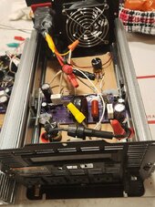
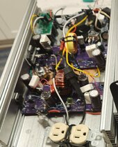
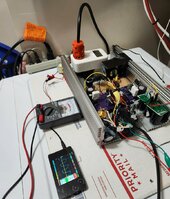
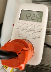
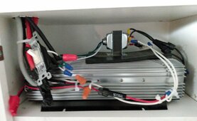
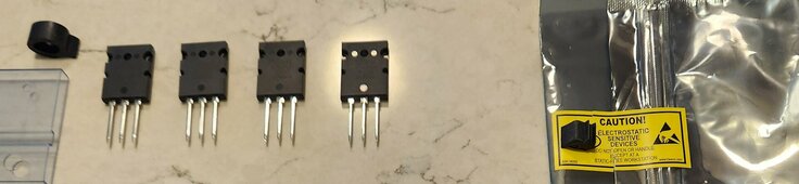
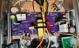
Interesting response: Testing new P & N MOSFETs Gate open/Gate close test at 100k resistance at just 9VDC.
No problems operating the gates, at no matter opening or closing the gate.
Only the P FET demonstrated a micro time delay on closing, Suggesting my 15K gate close resistors are wrong and a much better value is 40K on both FETs.
Good news is they both will respond the same to lower test voltages.
Back to the bench to swap out the gate close resistors to 40K, will be ready for full testing tomorrow.
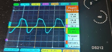
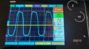
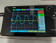
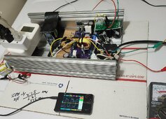
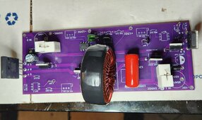
WOW before and after photos, was over driving the gates in both directions, Much better sine wave and power curve.
P FET is the top on the scope N channel on the bottom .
Can't wait to test.
More soon
No problems operating the gates, at no matter opening or closing the gate.
Only the P FET demonstrated a micro time delay on closing, Suggesting my 15K gate close resistors are wrong and a much better value is 40K on both FETs.
Good news is they both will respond the same to lower test voltages.
Back to the bench to swap out the gate close resistors to 40K, will be ready for full testing tomorrow.
WOW before and after photos, was over driving the gates in both directions, Much better sine wave and power curve.
P FET is the top on the scope N channel on the bottom .
Can't wait to test.
More soon
Attachments
Last edited:


 ️
️


")