diy solar

diy solar

DIY All-In-One Solar Generator - Control Board

Okey Guys,
apologies for being away all this while.
I'm in travel with limited connectivity, so please bear with me.
Lots of discussions going around, trying to sum them up w.r.t the design the way I understand them:).

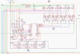
Few changes incorporated:
1) Transistor Opto(s) changed with Mosfet Opto(s).
2) R7 reduced to 4.7k.
3) Z1 Zener voltage Vz detected to verify PV state and activate charging functions (Through Digital Input).
4) Parallel Zeners(Z2) removed.
1599133625912.png

In Details:

I tried the regulator circuit in LTSpice with a couple substitutions using whatever was in the library.
Main problem I see is that 47k & 10k can't be at 12V unless Vpv > 68V
Using 47k pulldown seems to work. I does have a 5 ms time constant to turn off gate. Just so long as MOSFET has enough thermal mass to soak of the power dissipated in that time.


View attachment 20885

View attachment 20886
Thanks @Hedges , that's some nice simulation.
Could this be due to excess current leak through pulldown resistor?
If that's the case can we substitute R7 with a smaller resistor(like 4.7k) to bring up the Zener current which could as well help maintain better zener regulation as suggested by @Cal .

Vg = 35V * 10k/(47k + 10k) = 6.1V

The OP could be looking at a major disaster when on a cloudy day Vmp drops below 35V.

The correct way to design the zener circuit is for the bias resistor to account for the load current. Steady state load current is 12V/10k = 1.2 mA.
We'll include a buffer and say load current is 2 mA. Estimate min zener current at 5 mA. Not sure what the minimum Vmp can get down to? Estamate Vmp_min = 30V.

R7 = Vmp_min /( Iz_min + I_load)
R7 = 30V / (5 mA + 2 mA) = 4.2 k ohm

In addition, the second zener diode should be removed.
@Cal : Second zener removed on your insistence?.
Thanks for the calculations, they clear up things.
Now got a question for you: Iz would only exceed Iz(min) when Gates are active.
Since I'm now using Iz to verify PV state, can we connect a second pull down resistor from +ive end of capacitor C1 to enable sufficient Zener current leak to keep Zener regulation well above minimum levels?
 

Attachments

  • Schematic.pdf
    208.6 KB · Views: 4
Nice changes ;)

Now got a question for you: Iz would only exceed Iz(min) when Gates are active.
Since I'm now using Iz to verify PV state, can we connect a second pull down resistor from +ive end of capacitor C1 to enable sufficient Zener current leak to keep Zener regulation well above minimum levels?

That's the reverse. The zener is used as a shunt regulator here so its current will be lower when the load current is higher.
 
Since I'm now using Iz to verify PV state, can we connect a second pull down resistor from +ive end of capacitor C1 to enable sufficient Zener current leak to keep Zener regulation well above minimum levels?

Zener regulation should be fine now. Though you did add another load (0.8 mA) to R7. There goes the buffer I added.

You realize R7 need to be a 1/2 W resistor?
 
Okey Guys,
apologies for being away all this while.
I'm in travel with limited connectivity, so please bear with me.
Lots of discussions going around, trying to sum them up w.r.t the design the way I understand them:).

Few changes incorporated:
1) Transistor Opto(s) changed with Mosfet Opto(s).
2) R7 reduced to 4.7k.
3) Z1 Zener voltage Vz detected to verify PV state and activate charging functions (Through Digital Input).
4) Parallel Zeners(Z2) removed.

In Details:


Thanks @Hedges , that's some nice simulation.
Could this be due to excess current leak through pulldown resistor?
If that's the case can we substitute R7 with a smaller resistor(like 4.7k) to bring up the Zener current which could as well help maintain better zener regulation as suggested by @Cal .


@Cal : Second zener removed on your insistence?.
Thanks for the calculations, they clear up things.
Now got a question for you: Iz would only exceed Iz(min) when Gates are active.
Since I'm now using Iz to verify PV state, can we connect a second pull down resistor from +ive end of capacitor C1 to enable sufficient Zener current leak to keep Zener regulation well above minimum levels?

Yes, too low a pulldown resistor for the pull-up resistor.
Now that you've made pullup lower value, that fixes the voltage and makes circuit faster.

(45 Vpv - 12 Vz)^2/4.7k = 0.23 W dissipation in resistor. Almost a quarter watt, so 0.25W resistor would be OK only at room temperature. Use at least 0.5W resistor. (as Cal posted while I was writing more)

The opto TLP175A has absolute max 60V, so if PV is 45 Voc, that part is safe even if zener was open circuit.
In the event of an open circuit or a short somewhere, you might want additional protection from damage to the MOSFETs.
The parallel zener you removed would have done that for first zener open, but not for short across the resistor.
You can make the 4.7k out of two resistors in series, so if one is shorted the other gets cooked but voltage remains clamped.
You can still have two zener, maybe make second one 13V so it doesn't affect circuit unless first one goes open.
When I have a circuit attenuating high voltage I like to use two in series so assembly defect or shorting out with a probe tip doesn't kill the ICs.

You can add a PTC fuse in series with resistor. At overload (shorted resistor), that will change from 100's of ohms to 100's of kohms.
That will protect a device that conducts current (e.g. bipolar transistor, but not a capacitive load like MOSFET gate. High voltage would kill the gate without overheating PTC, so clamping voltage is the only way. But it can protect MOSFET source/drain from excessive current or power dissipation.

If you put the PTC electrically between PV panels and opto-isolator (or between optoisolator and gate of MOSFETs), but thermally attach it to heatsink of MOSFETs, then in the event they overheat that would switch them off. While low voltage doesn't happen at no load with low light, when charge controller draws current it could pull voltage low. Want to avoid conditions where Vgs is pulled halfway low due to Vpv being pulled low, to the point where watts are burned in the MOSFET. That is something to avoid doing, but PTC fuse could detect it thermally and latch off until things cool.

In a PCB design I put the PTC on copper pads above a buried copper trace connected to the hot node. With breadboard assembly you can use a leaded PTC, bend the leads and glue case to heatsink.
 
Almost a quarter watt, so 0.25W resistor would be OK only at room temperature.

Bet you would burn your finger if using a 1/4W resistor and dissipating 0.23W. Even at room temps.

Always, always derate resistors by 50%. 1/4W is not OK at room temps.
 
Bet you would burn your finger if using a 1/4W resistor and dissipating 0.23W. Even at room temps.

That's how I figured out the inductor in my RF matching circuit wasn't sized correctly. Value was correct but at elevated temperature the RF circuit became unstable.
Solution was to wind my RF transformer differently and only use series C no parallel L to match it.
Previously, the 0.2" square inductor had been half the impedance (carrying twice the current) of a 1" diameter transformer!

Sometimes we see designs with thru-hole 10W resistors standing a distance off the board, but the board is still browned under the resistor.

Here's an 0.25W SMT resistor, body size 0805 or 1206, 0.5W 1206 or 1210, all 155C.
Full power up to 70C, then linearly derated. 155 - 70 = 85C rise.
From ambient 25C, 85C rise reaches 110C.
As Cal said, you would burn your finger. It probably isn't hot enough to sizzle so no audible warning.


1599148462357.png
 
The parallel zener you removed would have done that for first zener open, but not for short across the resistor.
You can make the 4.7k out of two resistors in series, so if one is shorted the other gets cooked but voltage remains clamped.
You can still have two zener, maybe make second one 13V so it doesn't affect circuit unless first one goes open.
...

You can add a PTC fuse in series with resistor. At overload (shorted resistor), that will change from 100's of ohms to 100's of kohms.
That will protect a device that conducts current (e.g. bipolar transistor, but not a capacitive load like MOSFET gate. High voltage would kill the gate without overheating PTC, so clamping voltage is the only way. But it can protect MOSFET source/drain from excessive current or power dissipation.

If you put the PTC electrically between PV panels and opto-isolator (or between optoisolator and gate of MOSFETs), but thermally attach it to heatsink of MOSFETs, then in the event they overheat that would switch them off. While low voltage doesn't happen at no load with low light, when charge controller draws current it could pull voltage low. Want to avoid conditions where Vgs is pulled halfway low due to Vpv being pulled low, to the point where watts are burned in the MOSFET. That is something to avoid doing, but PTC fuse could detect it thermally and latch off until things cool.

In a PCB design I put the PTC on copper pads above a buried copper trace connected to the hot node. With breadboard assembly you can use a leaded PTC, bend the leads and glue case to heatsink.

Some brilliantly cleaver ideas @Hedges . Sound like pro design engineer at work.
Thanks for sharing them.

Let me incorporate changes and come back.
 
Back
Top